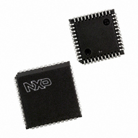
P87C591VFA/00,512 NXP Semiconductors, P87C591VFA/00,512 Datasheet - Page 40

P87C591VFA/00,512
Manufacturer Part Number
P87C591VFA/00,512
Description
IC 80C51 MCU 16K OTP 44-PLCC
Manufacturer
NXP Semiconductors
Series
87Cr
Datasheet
1.P87C591VFA00512.pdf
(160 pages)
Specifications of P87C591VFA/00,512
Core Processor
8051
Core Size
8-Bit
Speed
12MHz
Connectivity
CAN, EBI/EMI, I²C, UART/USART
Peripherals
POR, PWM, WDT
Number Of I /o
32
Program Memory Size
16KB (16K x 8)
Program Memory Type
OTP
Ram Size
512 x 8
Voltage - Supply (vcc/vdd)
4.75 V ~ 5.25 V
Data Converters
A/D 6x10b
Oscillator Type
Internal
Operating Temperature
-40°C ~ 85°C
Package / Case
44-PLCC
Processor Series
P87C5x
Core
80C51
Data Bus Width
8 bit
Data Ram Size
512 B
Interface Type
CAN, I2C, UART
Maximum Clock Frequency
12 MHz
Number Of Programmable I/os
32
Number Of Timers
3
Maximum Operating Temperature
+ 85 C
Mounting Style
SMD/SMT
3rd Party Development Tools
PK51, CA51, A51, ULINK2
Minimum Operating Temperature
- 40 C
On-chip Adc
10 bit, 6 Channel
Lead Free Status / RoHS Status
Lead free / RoHS Compliant
Eeprom Size
-
Lead Free Status / Rohs Status
Details
Other names
568-1256-5
935268182512
P87C591VFAA
935268182512
P87C591VFAA
Available stocks
Company
Part Number
Manufacturer
Quantity
Price
Company:
Part Number:
P87C591VFA/00,512
Manufacturer:
TI
Quantity:
8
Company:
Part Number:
P87C591VFA/00,512
Manufacturer:
NXP Semiconductors
Quantity:
10 000
Philips Semiconductors
12.5.7
The RIL register is used to define the receive interrupt level for the RXFIFO. A receive interrupt is generated if the number
of valid CAN message bytes in the RXFIFO exceeds the level specified in this register. Note that receive interrupts are
only generated if complete messages have been received. If RIL is set to 00 the PeliCAN functions like the receive
interrupt behaviour of the SJA1000.
Table 18 Bit interpretation of the Rx Interrupt Level (RIL)
12.5.8
The contents of the Bus Timing Register 0 defines the values of the Baud Rate Prescaler (BRP) and the Synchronization
Jump Width (SJW). This register can be accessed (read/write) if the Reset Mode is active. In Operating Mode, this
register is read only.
Table 19 Bus Timing Register 0 (BTR0) (CAN address 6)
12.5.8.1
The period of the CAN system clock t
is calculated using the following equation:
12.5.8.2
To compensate for phase shifts between clock oscillators of different bus controllers, any bus controller must
resynchronize on any relevant signal edge of the current transmission. The synchronization jump width defines the
maximum number of clock cycles a bit period may be shortened or lengthened by one resynchronization:
2000 Jul 26
Single-chip 8-bit microcontroller with CAN controller
SJW.1
RIL.7
7
7
CAN ADDR. 5
RX I
B
US
Baud Rate Prescaler (BRP)
Synchronization Jump Width (SJW)
NTERRUPT
T
IMING
SJW.0
t scl
RIL.6
6
R
6
EGISTER
L
=
EVEL
t CLK
(RIL)
0 (BTR0)
BRP.5
32 BRP.5
t CLK
RIL.5
5
scl
5
is programmable and determines the individual bit timing. The CAN system clock
=
t SJW
time period of the C´s system clock
+
16 BRP.4
=
BRP.4
RIL.4
t scl
4
4
2 SJW.1
+
40
8 BRP.3
RX INTERRUPT LEVEL (RIL)
BRP.3
RIL.3
3
+
3
SJW.0
+
4 BRP.2
+
1
BRP.2
=
+
RIL.2
-------------- -
f CLK
2 BRP.1
2
2
1
+
BRP.0
BRP.1
Preliminary Specification
RIL.1
1
1
+
1
P8xC591
BRP.0
RIL.0
0
0


