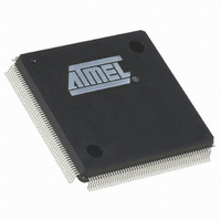
AT91SAM9XE128-QU Atmel, AT91SAM9XE128-QU Datasheet - Page 95

AT91SAM9XE128-QU
Manufacturer Part Number
AT91SAM9XE128-QU
Description
MCU ARM9 128K FLASH 208-PQFP
Manufacturer
Atmel
Series
AT91SAMr
Specifications of AT91SAM9XE128-QU
Core Processor
ARM9
Core Size
16/32-Bit
Speed
180MHz
Connectivity
EBI/EMI, Ethernet, I²C, MMC, SPI, SSC, UART/USART, USB
Peripherals
Brown-out Detect/Reset, POR, PWM, WDT
Number Of I /o
96
Program Memory Size
128KB (128K x 8)
Program Memory Type
FLASH
Ram Size
40K x 8
Voltage - Supply (vcc/vdd)
1.65 V ~ 1.95 V
Data Converters
A/D 4x10b
Oscillator Type
Internal
Operating Temperature
-40°C ~ 85°C
Package / Case
208-MQFP, 208-PQFP
Processor Series
AT91SAMx
Core
ARM926EJ-S
Data Bus Width
32 bit
Data Ram Size
16 KB
Interface Type
2-Wire, EBI, I2S, SPI, USART
Maximum Clock Frequency
180 MHz
Number Of Programmable I/os
96
Number Of Timers
6
Maximum Operating Temperature
+ 85 C
Mounting Style
SMD/SMT
3rd Party Development Tools
JTRACE-ARM-2M, KSK-AT91SAM9XE-PL, MDK-ARM, RL-ARM, ULINK2
Development Tools By Supplier
AT91SAM-ICE, AT91-ISP, AT91SAM9XE-EK
Minimum Operating Temperature
- 40 C
On-chip Adc
10 bit, 4 Channel
For Use With
AT91SAM9XE-EK - KIT EVAL FOR AT91SAM9XEAT91SAM-ICE - EMULATOR FOR AT91 ARM7/ARM9
Lead Free Status / RoHS Status
Lead free / RoHS Compliant
Eeprom Size
-
Lead Free Status / Rohs Status
Lead free / RoHS Compliant
Available stocks
Company
Part Number
Manufacturer
Quantity
Price
- Current page: 95 of 860
- Download datasheet (13Mb)
Table 14-17. Signal Description List (Continued)
14.3.2
6254C–ATARM–22-Jan-10
Signal Name
TST
PGMEN0
PGMEN1
PGMEN2
PGMEN3
TCK
TDI
TDO
TMS
Entering Serial Programming Mode
Function
Test Mode Select
Test Mode Select
Test Mode Select
Test Mode Select
Test Mode Select
JTAG TCK
JTAG Test Data In
JTAG Test Data Out
JTAG Test Mode Select
The following algorithm puts the device in Serial Programming Mode:
Note:
Table 14-18. Reset TAP Controller and Go to Select-DR-Scan
• Apply GND, VDDIO, VDDCORE and VDDPLL.
• Apply XIN clock within T
• Wait for T
• Reset the TAP controller clocking 5 TCK pulses with TMS set.
• Shift 0x2 into the IR register (IR is 4 bits long, LSB first) without going through the Run-Test-
• Shift 0x2 into the DR register (DR is 4 bits long, LSB first) without going through the Run-
• Shift 0xC into the IR register (IR is 4 bits long, LSB first) without going through the Run-Test-
Idle state.
Test-Idle state.
Idle state.
After reset, the device is clocked by the internal RC oscillator. Before clearing RDY signal, if an
external clock ( > 32 kHz) is connected to XIN, then the device will switch on the external clock.
Else, XIN input is not considered. An higher frequency on XIN speeds up the programmer
handshake.
TDI
POR_RESET
Xt
X
X
X
X
X
X
.
AT91SAM9XE128/256/512 Preliminary
POR_RESET
JTAG
Test
TMS
1
1
1
1
1
0
1
+ 32(T
Output
Type
Input
Input
Input
Input
Input
Input
Input
Input
TAP Controller State
Test-Logic Reset
Run-Test/Idle
Select-DR-Scan
SCLK
) if an external clock is available.
Active
Level
High
High
High
Low
Low
-
-
-
-
Comments
Must be connected to VDDBU.
Must be connected to VDDIO
Must be connected to VDDIO
Must be connected to GND
Must be connected to GND
Pulled-up input at reset
Pulled-up input at reset
Pulled-up input at reset
95
Related parts for AT91SAM9XE128-QU
Image
Part Number
Description
Manufacturer
Datasheet
Request
R

Part Number:
Description:
KIT EVAL FOR AT91SAM9XE
Manufacturer:
Atmel
Datasheet:

Part Number:
Description:
MCU ARM9 64K SRAM 144-LFBGA
Manufacturer:
Atmel
Datasheet:

Part Number:
Description:
IC ARM7 MCU FLASH 256K 100LQFP
Manufacturer:
Atmel
Datasheet:

Part Number:
Description:
IC ARM9 MPU 217-LFBGA
Manufacturer:
Atmel
Datasheet:

Part Number:
Description:
MCU ARM9 ULTRA LOW PWR 217-LFBGA
Manufacturer:
Atmel
Datasheet:

Part Number:
Description:
MCU ARM9 324-TFBGA
Manufacturer:
Atmel
Datasheet:

Part Number:
Description:
IC MCU ARM9 SAMPLING 217CBGA
Manufacturer:
Atmel
Datasheet:

Part Number:
Description:
IC ARM9 MCU 217-LFBGA
Manufacturer:
Atmel
Datasheet:

Part Number:
Description:
IC ARM9 MCU 208-PQFP
Manufacturer:
Atmel
Datasheet:

Part Number:
Description:
MCU ARM 512K HS FLASH 100-LQFP
Manufacturer:
Atmel
Datasheet:

Part Number:
Description:
MCU ARM 512K HS FLASH 100-TFBGA
Manufacturer:
Atmel
Datasheet:

Part Number:
Description:
IC ARM9 MCU 200 MHZ 324-TFBGA
Manufacturer:
Atmel
Datasheet:

Part Number:
Description:
IC ARM MCU 16BIT 128K 256BGA
Manufacturer:
Atmel
Datasheet:

Part Number:
Description:
IC ARM7 MCU 32BIT 128K 64LQFP
Manufacturer:
Atmel
Datasheet:

Part Number:
Description:
IC ARM7 MCU FLASH 256K 128-LQFP
Manufacturer:
Atmel
Datasheet:


