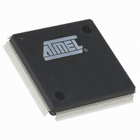
AT91SAM9XE128-QU Atmel, AT91SAM9XE128-QU Datasheet - Page 92

AT91SAM9XE128-QU
Manufacturer Part Number
AT91SAM9XE128-QU
Description
MCU ARM9 128K FLASH 208-PQFP
Manufacturer
Atmel
Series
AT91SAMr
Specifications of AT91SAM9XE128-QU
Core Processor
ARM9
Core Size
16/32-Bit
Speed
180MHz
Connectivity
EBI/EMI, Ethernet, I²C, MMC, SPI, SSC, UART/USART, USB
Peripherals
Brown-out Detect/Reset, POR, PWM, WDT
Number Of I /o
96
Program Memory Size
128KB (128K x 8)
Program Memory Type
FLASH
Ram Size
40K x 8
Voltage - Supply (vcc/vdd)
1.65 V ~ 1.95 V
Data Converters
A/D 4x10b
Oscillator Type
Internal
Operating Temperature
-40°C ~ 85°C
Package / Case
208-MQFP, 208-PQFP
Processor Series
AT91SAMx
Core
ARM926EJ-S
Data Bus Width
32 bit
Data Ram Size
16 KB
Interface Type
2-Wire, EBI, I2S, SPI, USART
Maximum Clock Frequency
180 MHz
Number Of Programmable I/os
96
Number Of Timers
6
Maximum Operating Temperature
+ 85 C
Mounting Style
SMD/SMT
3rd Party Development Tools
JTRACE-ARM-2M, KSK-AT91SAM9XE-PL, MDK-ARM, RL-ARM, ULINK2
Development Tools By Supplier
AT91SAM-ICE, AT91-ISP, AT91SAM9XE-EK
Minimum Operating Temperature
- 40 C
On-chip Adc
10 bit, 4 Channel
For Use With
AT91SAM9XE-EK - KIT EVAL FOR AT91SAM9XEAT91SAM-ICE - EMULATOR FOR AT91 ARM7/ARM9
Lead Free Status / RoHS Status
Lead free / RoHS Compliant
Eeprom Size
-
Lead Free Status / Rohs Status
Lead free / RoHS Compliant
Available stocks
Company
Part Number
Manufacturer
Quantity
Price
- Current page: 92 of 860
- Download datasheet (13Mb)
14.2.5.6
14.2.5.7
92
AT91SAM9XE128/256/512 Preliminary
Flash Security Bit Command
Memory Write Command
General-purpose NVM bits can be read using the Get GPNVM Bit command (GGPB). The n
GP NVM bit is active when bit n of the bit mask is set..
Table 14-13. Get GP NVM Bit Command
A security bit can be set using the Set Security Bit command (SSE). Once the security bit is
active, the Fast Flash programming is disabled. No other command can be run. An event on the
Erase pin can erase the security bit once the contents of the Flash have been erased.
Table 14-14. Set Security Bit Command
Once the security bit is set, it is not possible to access FFPI. The only way to erase the security
bit is to erase the Flash.
In order to erase the Flash, the user must perform the following:
Then it is possible to return to FFPI mode and check that Flash is erased.
This command is used to perform a write access to any memory location.
The Memory Write command (WRAM) is optimized for consecutive writes. Write handshaking
can be chained; an internal address buffer is automatically increased.
Table 14-15. Write Command
Step
1
2
Step
1
2
Step
1
2
3
4
5
...
n
• Power-off the chip
• Power-on the chip with TST = 0
• Assert Erase during a period of more than 220 ms
• Power-off the chip
Handshake Sequence
Write handshaking
Read handshaking
Handshake Sequence
Write handshaking
Write handshaking
Handshake Sequence
Write handshaking
Write handshaking
Write handshaking
Write handshaking
Write handshaking
...
Write handshaking
MODE[3:0]
CMDE
ADDR0
ADDR1
DATA
DATA
...
ADDR0
MODE[3:0]
CMDE
DATA
MODE[3:0]
CMDE
DATA
DATA[15:0]
WRAM
Memory Address LSB
Memory Address
*Memory Address++
*Memory Address++
...
Memory Address LSB
DATA[15:0]
SSE
0
DATA[15:0]
GGPB
GP NVM Bit Mask Status
0 = GP NVM bit is cleared
1 = GP NVM bit is set
6254C–ATARM–22-Jan-10
th
Related parts for AT91SAM9XE128-QU
Image
Part Number
Description
Manufacturer
Datasheet
Request
R

Part Number:
Description:
KIT EVAL FOR AT91SAM9XE
Manufacturer:
Atmel
Datasheet:

Part Number:
Description:
MCU ARM9 64K SRAM 144-LFBGA
Manufacturer:
Atmel
Datasheet:

Part Number:
Description:
IC ARM7 MCU FLASH 256K 100LQFP
Manufacturer:
Atmel
Datasheet:

Part Number:
Description:
IC ARM9 MPU 217-LFBGA
Manufacturer:
Atmel
Datasheet:

Part Number:
Description:
MCU ARM9 ULTRA LOW PWR 217-LFBGA
Manufacturer:
Atmel
Datasheet:

Part Number:
Description:
MCU ARM9 324-TFBGA
Manufacturer:
Atmel
Datasheet:

Part Number:
Description:
IC MCU ARM9 SAMPLING 217CBGA
Manufacturer:
Atmel
Datasheet:

Part Number:
Description:
IC ARM9 MCU 217-LFBGA
Manufacturer:
Atmel
Datasheet:

Part Number:
Description:
IC ARM9 MCU 208-PQFP
Manufacturer:
Atmel
Datasheet:

Part Number:
Description:
MCU ARM 512K HS FLASH 100-LQFP
Manufacturer:
Atmel
Datasheet:

Part Number:
Description:
MCU ARM 512K HS FLASH 100-TFBGA
Manufacturer:
Atmel
Datasheet:

Part Number:
Description:
IC ARM9 MCU 200 MHZ 324-TFBGA
Manufacturer:
Atmel
Datasheet:

Part Number:
Description:
IC ARM MCU 16BIT 128K 256BGA
Manufacturer:
Atmel
Datasheet:

Part Number:
Description:
IC ARM7 MCU 32BIT 128K 64LQFP
Manufacturer:
Atmel
Datasheet:

Part Number:
Description:
IC ARM7 MCU FLASH 256K 128-LQFP
Manufacturer:
Atmel
Datasheet:


