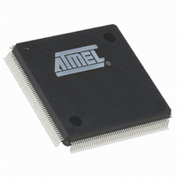
AT91SAM9XE128-QU Atmel, AT91SAM9XE128-QU Datasheet - Page 738

AT91SAM9XE128-QU
Manufacturer Part Number
AT91SAM9XE128-QU
Description
MCU ARM9 128K FLASH 208-PQFP
Manufacturer
Atmel
Series
AT91SAMr
Specifications of AT91SAM9XE128-QU
Core Processor
ARM9
Core Size
16/32-Bit
Speed
180MHz
Connectivity
EBI/EMI, Ethernet, I²C, MMC, SPI, SSC, UART/USART, USB
Peripherals
Brown-out Detect/Reset, POR, PWM, WDT
Number Of I /o
96
Program Memory Size
128KB (128K x 8)
Program Memory Type
FLASH
Ram Size
40K x 8
Voltage - Supply (vcc/vdd)
1.65 V ~ 1.95 V
Data Converters
A/D 4x10b
Oscillator Type
Internal
Operating Temperature
-40°C ~ 85°C
Package / Case
208-MQFP, 208-PQFP
Processor Series
AT91SAMx
Core
ARM926EJ-S
Data Bus Width
32 bit
Data Ram Size
16 KB
Interface Type
2-Wire, EBI, I2S, SPI, USART
Maximum Clock Frequency
180 MHz
Number Of Programmable I/os
96
Number Of Timers
6
Maximum Operating Temperature
+ 85 C
Mounting Style
SMD/SMT
3rd Party Development Tools
JTRACE-ARM-2M, KSK-AT91SAM9XE-PL, MDK-ARM, RL-ARM, ULINK2
Development Tools By Supplier
AT91SAM-ICE, AT91-ISP, AT91SAM9XE-EK
Minimum Operating Temperature
- 40 C
On-chip Adc
10 bit, 4 Channel
For Use With
AT91SAM9XE-EK - KIT EVAL FOR AT91SAM9XEAT91SAM-ICE - EMULATOR FOR AT91 ARM7/ARM9
Lead Free Status / RoHS Status
Lead free / RoHS Compliant
Eeprom Size
-
Lead Free Status / Rohs Status
Lead free / RoHS Compliant
Available stocks
Company
Part Number
Manufacturer
Quantity
Price
- Current page: 738 of 860
- Download datasheet (13Mb)
39.6.10
Register Name:
Address:
Access Type:
WARNING: Due to synchronization between MCK and UDPCK, the software application must wait for the end of the write
operation before executing another write by polling the bits which must be set/cleared.
Note:
• TXCOMP: Generates an IN Packet with Data Previously Written in the DPR
This flag generates an interrupt while it is set to one.
Write (Cleared by the firmware):
0 = Clear the flag, clear the interrupt.
1 = No effect.
Read (Set by the USB peripheral):
0 = Data IN transaction has not been acknowledged by the Host.
1 = Data IN transaction is achieved, acknowledged by the Host.
After having issued a Data IN transaction setting TXPKTRDY, the device firmware waits for TXCOMP to be sure that the
host has acknowledged the transaction.
738
//! Clear flags of UDP UDP_CSR register and waits for synchronization
#define Udp_ep_clr_flag(pInterface, endpoint, flags) { \
//! Set flags of UDP UDP_CSR register and waits for synchronization
#define Udp_ep_set_flag(pInterface, endpoint, flags) { \
EPEDS
DIR
31
23
15
–
7
pInterface->UDP_CSR[endpoint] &= ~(flags); \
while ( (pInterface->UDP_CSR[endpoint] & (flags)) == (flags) ); \
}
pInterface->UDP_CSR[endpoint] |= (flags); \
while ( (pInterface->UDP_CSR[endpoint] & (flags)) != (flags) ); \
}
In a preemptive environment, set or clear the flag and wait for a time of 1 UDPCK clock cycle and 1peripheral clock cycle. How-
ever, RX_DATA_BLK0, TXPKTRDY, RX_DATA_BK1 require wait times of 3 UDPCK clock cycles and 3 peripheral clock cycles
before accessing DPR.
AT91SAM9XE128/256/512 Preliminary
UDP Endpoint Control and Status Register
RX_DATA_
BK1
30
22
14
UDP_CSRx [x = 0..5]
0xFFFA402C
–
–
6
Read-write
FORCE
STALL
29
21
13
–
–
5
TXPKTRDY
28
20
12
–
–
4
RXBYTECNT
STALLSENT
ISOERROR
DTGLE
27
19
11
–
3
RXSETUP
26
18
10
2
RXBYTECNT
RX_DATA_
EPTYPE
BK0
25
17
9
1
6254C–ATARM–22-Jan-10
TXCOMP
24
16
8
0
Related parts for AT91SAM9XE128-QU
Image
Part Number
Description
Manufacturer
Datasheet
Request
R

Part Number:
Description:
KIT EVAL FOR AT91SAM9XE
Manufacturer:
Atmel
Datasheet:

Part Number:
Description:
MCU ARM9 64K SRAM 144-LFBGA
Manufacturer:
Atmel
Datasheet:

Part Number:
Description:
IC ARM7 MCU FLASH 256K 100LQFP
Manufacturer:
Atmel
Datasheet:

Part Number:
Description:
IC ARM9 MPU 217-LFBGA
Manufacturer:
Atmel
Datasheet:

Part Number:
Description:
MCU ARM9 ULTRA LOW PWR 217-LFBGA
Manufacturer:
Atmel
Datasheet:

Part Number:
Description:
MCU ARM9 324-TFBGA
Manufacturer:
Atmel
Datasheet:

Part Number:
Description:
IC MCU ARM9 SAMPLING 217CBGA
Manufacturer:
Atmel
Datasheet:

Part Number:
Description:
IC ARM9 MCU 217-LFBGA
Manufacturer:
Atmel
Datasheet:

Part Number:
Description:
IC ARM9 MCU 208-PQFP
Manufacturer:
Atmel
Datasheet:

Part Number:
Description:
MCU ARM 512K HS FLASH 100-LQFP
Manufacturer:
Atmel
Datasheet:

Part Number:
Description:
MCU ARM 512K HS FLASH 100-TFBGA
Manufacturer:
Atmel
Datasheet:

Part Number:
Description:
IC ARM9 MCU 200 MHZ 324-TFBGA
Manufacturer:
Atmel
Datasheet:

Part Number:
Description:
IC ARM MCU 16BIT 128K 256BGA
Manufacturer:
Atmel
Datasheet:

Part Number:
Description:
IC ARM7 MCU 32BIT 128K 64LQFP
Manufacturer:
Atmel
Datasheet:

Part Number:
Description:
IC ARM7 MCU FLASH 256K 128-LQFP
Manufacturer:
Atmel
Datasheet:


