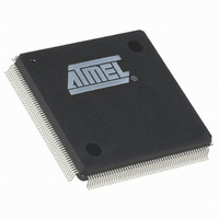
AT91SAM9XE128-QU Atmel, AT91SAM9XE128-QU Datasheet - Page 632

AT91SAM9XE128-QU
Manufacturer Part Number
AT91SAM9XE128-QU
Description
MCU ARM9 128K FLASH 208-PQFP
Manufacturer
Atmel
Series
AT91SAMr
Specifications of AT91SAM9XE128-QU
Core Processor
ARM9
Core Size
16/32-Bit
Speed
180MHz
Connectivity
EBI/EMI, Ethernet, I²C, MMC, SPI, SSC, UART/USART, USB
Peripherals
Brown-out Detect/Reset, POR, PWM, WDT
Number Of I /o
96
Program Memory Size
128KB (128K x 8)
Program Memory Type
FLASH
Ram Size
40K x 8
Voltage - Supply (vcc/vdd)
1.65 V ~ 1.95 V
Data Converters
A/D 4x10b
Oscillator Type
Internal
Operating Temperature
-40°C ~ 85°C
Package / Case
208-MQFP, 208-PQFP
Processor Series
AT91SAMx
Core
ARM926EJ-S
Data Bus Width
32 bit
Data Ram Size
16 KB
Interface Type
2-Wire, EBI, I2S, SPI, USART
Maximum Clock Frequency
180 MHz
Number Of Programmable I/os
96
Number Of Timers
6
Maximum Operating Temperature
+ 85 C
Mounting Style
SMD/SMT
3rd Party Development Tools
JTRACE-ARM-2M, KSK-AT91SAM9XE-PL, MDK-ARM, RL-ARM, ULINK2
Development Tools By Supplier
AT91SAM-ICE, AT91-ISP, AT91SAM9XE-EK
Minimum Operating Temperature
- 40 C
On-chip Adc
10 bit, 4 Channel
For Use With
AT91SAM9XE-EK - KIT EVAL FOR AT91SAM9XEAT91SAM-ICE - EMULATOR FOR AT91 ARM7/ARM9
Lead Free Status / RoHS Status
Lead free / RoHS Compliant
Eeprom Size
-
Lead Free Status / Rohs Status
Lead free / RoHS Compliant
Available stocks
Company
Part Number
Manufacturer
Quantity
Price
- Current page: 632 of 860
- Download datasheet (13Mb)
37.7.2
37.7.3
6254C–ATARM–22-Jan-10
Data Transfer Operation
Read Operation
The MultiMedia Card allows several read/write operations (single block, multiple blocks, stream,
etc.). These kind of transfers can be selected setting the Transfer Type (TRTYP) field in the MCI
Command Register (MCI_CMDR).
These operations can be done using the features of the Peripheral DMA Controller (PDC). If the
PDCMODE bit is set in MCI_MR, then all reads and writes use the PDC facilities.
In all cases, the block length (BLKLEN field) must be defined either in the mode register
MCI_MR, or in the Block Register MCI_BLKR. This field determines the size of the data block.
Enabling PDC Force Byte Transfer (PDCFBYTE bit in the MCI_MR) allows the PDC to manage
with internal byte transfers, so that transfer of blocks with a size different from modulo 4 can be
supported. When PDC Force Byte Transfer is disabled, the PDC type of transfers are in words,
otherwise the type of transfers are in bytes.
Consequent to MMC Specification 3.1, two types of multiple block read (or write) transactions
are defined (the host can use either one at any time):
The following flowchart shows how to read a single block with or without use of PDC facilities. In
this example (see
the user can configure the interrupt enable register (MCI_IER) to trigger an interrupt at the end
of read.
• Open-ended/Infinite Multiple block read (or write):
• Multiple block read (or write) with pre-defined block count (since version 3.1 and higher):
The number of blocks for the read (or write) multiple block operation is not defined. The card
will continuously transfer (or program) data blocks until a stop transmission command is
received.
The card will transfer (or program) the requested number of data blocks and terminate the
transaction. The stop command is not required at the end of this type of multiple block read
(or write), unless terminated with an error. In order to start a multiple block read (or write)
with pre-defined block count, the host must correctly program the MCI Block Register
(MCI_BLKR). Otherwise the card will start an open-ended multiple block read. The BCNT
field of the Block Register defines the number of blocks to transfer (from 1 to 65535 blocks).
Programming the value 0 in the BCNT field corresponds to an infinite block transfer.
Figure
AT91SAM9XE128/256/512 Preliminary
37-10), a polling method is used to wait for the end of read. Similarly,
632
Related parts for AT91SAM9XE128-QU
Image
Part Number
Description
Manufacturer
Datasheet
Request
R

Part Number:
Description:
KIT EVAL FOR AT91SAM9XE
Manufacturer:
Atmel
Datasheet:

Part Number:
Description:
MCU ARM9 64K SRAM 144-LFBGA
Manufacturer:
Atmel
Datasheet:

Part Number:
Description:
IC ARM7 MCU FLASH 256K 100LQFP
Manufacturer:
Atmel
Datasheet:

Part Number:
Description:
IC ARM9 MPU 217-LFBGA
Manufacturer:
Atmel
Datasheet:

Part Number:
Description:
MCU ARM9 ULTRA LOW PWR 217-LFBGA
Manufacturer:
Atmel
Datasheet:

Part Number:
Description:
MCU ARM9 324-TFBGA
Manufacturer:
Atmel
Datasheet:

Part Number:
Description:
IC MCU ARM9 SAMPLING 217CBGA
Manufacturer:
Atmel
Datasheet:

Part Number:
Description:
IC ARM9 MCU 217-LFBGA
Manufacturer:
Atmel
Datasheet:

Part Number:
Description:
IC ARM9 MCU 208-PQFP
Manufacturer:
Atmel
Datasheet:

Part Number:
Description:
MCU ARM 512K HS FLASH 100-LQFP
Manufacturer:
Atmel
Datasheet:

Part Number:
Description:
MCU ARM 512K HS FLASH 100-TFBGA
Manufacturer:
Atmel
Datasheet:

Part Number:
Description:
IC ARM9 MCU 200 MHZ 324-TFBGA
Manufacturer:
Atmel
Datasheet:

Part Number:
Description:
IC ARM MCU 16BIT 128K 256BGA
Manufacturer:
Atmel
Datasheet:

Part Number:
Description:
IC ARM7 MCU 32BIT 128K 64LQFP
Manufacturer:
Atmel
Datasheet:

Part Number:
Description:
IC ARM7 MCU FLASH 256K 128-LQFP
Manufacturer:
Atmel
Datasheet:


