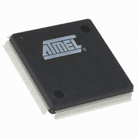
AT91SAM9XE128-QU Atmel, AT91SAM9XE128-QU Datasheet - Page 6

AT91SAM9XE128-QU
Manufacturer Part Number
AT91SAM9XE128-QU
Description
MCU ARM9 128K FLASH 208-PQFP
Manufacturer
Atmel
Series
AT91SAMr
Specifications of AT91SAM9XE128-QU
Core Processor
ARM9
Core Size
16/32-Bit
Speed
180MHz
Connectivity
EBI/EMI, Ethernet, I²C, MMC, SPI, SSC, UART/USART, USB
Peripherals
Brown-out Detect/Reset, POR, PWM, WDT
Number Of I /o
96
Program Memory Size
128KB (128K x 8)
Program Memory Type
FLASH
Ram Size
40K x 8
Voltage - Supply (vcc/vdd)
1.65 V ~ 1.95 V
Data Converters
A/D 4x10b
Oscillator Type
Internal
Operating Temperature
-40°C ~ 85°C
Package / Case
208-MQFP, 208-PQFP
Processor Series
AT91SAMx
Core
ARM926EJ-S
Data Bus Width
32 bit
Data Ram Size
16 KB
Interface Type
2-Wire, EBI, I2S, SPI, USART
Maximum Clock Frequency
180 MHz
Number Of Programmable I/os
96
Number Of Timers
6
Maximum Operating Temperature
+ 85 C
Mounting Style
SMD/SMT
3rd Party Development Tools
JTRACE-ARM-2M, KSK-AT91SAM9XE-PL, MDK-ARM, RL-ARM, ULINK2
Development Tools By Supplier
AT91SAM-ICE, AT91-ISP, AT91SAM9XE-EK
Minimum Operating Temperature
- 40 C
On-chip Adc
10 bit, 4 Channel
For Use With
AT91SAM9XE-EK - KIT EVAL FOR AT91SAM9XEAT91SAM-ICE - EMULATOR FOR AT91 ARM7/ARM9
Lead Free Status / RoHS Status
Lead free / RoHS Compliant
Eeprom Size
-
Lead Free Status / Rohs Status
Lead free / RoHS Compliant
Available stocks
Company
Part Number
Manufacturer
Quantity
Price
- Current page: 6 of 860
- Download datasheet (13Mb)
3. Signal Description
Table 3-1.
6
Signal Name
VDDIOM
VDDIOP0
VDDIOP1
VDDBU
VDDANA
VDDPLL
VDDCORE
GND
GNDPLL
GNDANA
GNDBU
XIN
XOUT
XIN32
XOUT32
OSCSEL
PLLRCA
PCK0 - PCK1
SHDN
WKUP
NTRST
TCK
TDI
TDO
TMS
JTAGSEL
RTCK
AT91SAM9XE128/256/512 Preliminary
Signal Description List
Function
EBI I/O Lines Power Supply
Peripherals I/O Lines Power Supply
Peripherals I/O Lines Power Supply
Backup I/O Lines Power Supply
Analog Power Supply
PLL Power Supply
Core Chip and Embedded Memories
Power Supply
Ground
PLL Ground
Analog Ground
Backup Ground
Main Oscillator Input
Main Oscillator Output
Slow Clock Oscillator Input
Slow Clock Oscillator Output
Slow Clock Oscillator Selection
PLL A Filter
Programmable Clock Output
Shutdown Control
Wake-Up Input
Test Reset Signal
Test Clock
Test Data In
Test Data Out
Test Mode Select
JTAG Selection
Return Test Clock
Table 3-1
gives details on the signal name classified by peripheral.
Clocks, Oscillators and PLLs
Shutdown, Wakeup Logic
Power Supplies
ICE and JTAG
Ground
Ground
Ground
Ground
Output
Output
Output
Output
Output
Output
Power
Power
Power
Power
Power
Power
Power
Type
Input
Input
Input
Input
Input
Input
Input
Input
Input
Input
Active
Level
Low
Low
Reference
VDDIOP0
VDDIOP0
VDDIOP0
VDDIOP0
VDDIOP0
VDDIOP0
Voltage
VDDBU
VDDBU
VDDBU
VDDBU
(2)
Comments
1.65V to 1.95V or 3.0V to 3.6V
3.0V to 3.6V
1.65V to 3.6V
1.65V to 1.95V
3.0V to 3.6V
1.65V to 1.95V
1.65V to 1.95V
Accepts between 0V and
VDDBU.
Driven at 0V only.
Accepts between 0V and VDDBU.
Pull-Up resistor (100 k
No pull-up resistor, Schmitt
trigger
No pull-up resistor, Schmitt
trigger
No pull-up resistor, Schmitt
trigger
Pull-down resistor (15 k
6254C–ATARM–22-Jan-10
Ω
Ω
)
).
Related parts for AT91SAM9XE128-QU
Image
Part Number
Description
Manufacturer
Datasheet
Request
R

Part Number:
Description:
KIT EVAL FOR AT91SAM9XE
Manufacturer:
Atmel
Datasheet:

Part Number:
Description:
MCU ARM9 64K SRAM 144-LFBGA
Manufacturer:
Atmel
Datasheet:

Part Number:
Description:
IC ARM7 MCU FLASH 256K 100LQFP
Manufacturer:
Atmel
Datasheet:

Part Number:
Description:
IC ARM9 MPU 217-LFBGA
Manufacturer:
Atmel
Datasheet:

Part Number:
Description:
MCU ARM9 ULTRA LOW PWR 217-LFBGA
Manufacturer:
Atmel
Datasheet:

Part Number:
Description:
MCU ARM9 324-TFBGA
Manufacturer:
Atmel
Datasheet:

Part Number:
Description:
IC MCU ARM9 SAMPLING 217CBGA
Manufacturer:
Atmel
Datasheet:

Part Number:
Description:
IC ARM9 MCU 217-LFBGA
Manufacturer:
Atmel
Datasheet:

Part Number:
Description:
IC ARM9 MCU 208-PQFP
Manufacturer:
Atmel
Datasheet:

Part Number:
Description:
MCU ARM 512K HS FLASH 100-LQFP
Manufacturer:
Atmel
Datasheet:

Part Number:
Description:
MCU ARM 512K HS FLASH 100-TFBGA
Manufacturer:
Atmel
Datasheet:

Part Number:
Description:
IC ARM9 MCU 200 MHZ 324-TFBGA
Manufacturer:
Atmel
Datasheet:

Part Number:
Description:
IC ARM MCU 16BIT 128K 256BGA
Manufacturer:
Atmel
Datasheet:

Part Number:
Description:
IC ARM7 MCU 32BIT 128K 64LQFP
Manufacturer:
Atmel
Datasheet:

Part Number:
Description:
IC ARM7 MCU FLASH 256K 128-LQFP
Manufacturer:
Atmel
Datasheet:


