DSPIC33FJ32GS406-I/PT Microchip Technology, DSPIC33FJ32GS406-I/PT Datasheet - Page 338
DSPIC33FJ32GS406-I/PT
Manufacturer Part Number
DSPIC33FJ32GS406-I/PT
Description
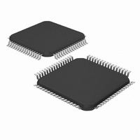
IC MCU/DSP 32KB FLASH 64TQFP
Manufacturer
Microchip Technology
Series
dsPIC™ 33Fr
Specifications of DSPIC33FJ32GS406-I/PT
Core Processor
dsPIC
Core Size
16-Bit
Speed
40 MIPs
Connectivity
I²C, IrDA, LIN, SCI, SPI, UART/USART, USB
Peripherals
Brown-out Detect/Reset, QEI, POR, PWM, WDT
Number Of I /o
58
Program Memory Size
32KB (32K x 8)
Program Memory Type
FLASH
Ram Size
4K x 8
Voltage - Supply (vcc/vdd)
3 V ~ 3.6 V
Data Converters
A/D 16x10b
Oscillator Type
Internal
Operating Temperature
-40°C ~ 85°C
Package / Case
64-TFQFP
Core Frequency
40MHz
Embedded Interface Type
I2C, SPI, UART
No. Of I/o's
53
Flash Memory Size
32KB
Supply Voltage Range
3V To 3.6V
Rohs Compliant
Yes
Lead Free Status / RoHS Status
Lead free / RoHS Compliant
Eeprom Size
-
Lead Free Status / RoHS Status
Lead free / RoHS Compliant, Lead free / RoHS Compliant
Available stocks
Company
Part Number
Manufacturer
Quantity
Price
Company:

Part Number:
DSPIC33FJ32GS406-I/PT
Manufacturer:
Microchip Technology
Quantity:
10 000


dsPIC33FJ32GS406/606/608/610 and dsPIC33FJ64GS406/606/608/610
FIGURE 24-2:
24.5
dsPIC33FJ32GS406/606/608/610
dsPIC33FJ64GS406/606/608/610 devices implement
a JTAG interface, which supports boundary scan
device testing, as well as in-circuit programming.
Detailed information on this interface will be provided in
future revisions of the document.
24.6
dsPIC33FJ32GS406/606/608/610
dsPIC33FJ64GS406/606/608/610 family digital signal
controllers can be serially programmed while in the end
application circuit. This is done with two lines for clock
and data and three other lines for power, ground and
the programming sequence. Serial programming
allows
unprogrammed devices and then program the digital
signal controller just before shipping the product. Serial
programming also allows the most recent firmware or a
custom firmware to be programmed. Refer to the
“dsPIC33F/PIC24H Flash Programming Specification”
(DS70152)
Programming (ICSP).
Any of the three pairs of programming clock/data pins
can be used:
• PGEC1 and PGED1
• PGEC2 and PGED2
• PGEC3 and PGED3
DS70591C-page 338
All Device Resets
Transition to New Clock Source
Exit Sleep or Idle Mode
PWRSAV Instruction
CLRWDT Instruction
SWDTEN
FWDTEN
LPRC Clock
customers
JTAG Interface
In-Circuit Serial Programming
for
WINDIS
details
to
WDT BLOCK DIAGRAM
manufacture
about
In-Circuit
(Divide by N1)
WDTPRE
Prescaler
boards
RS
WDT Window Select
Serial
with
and
and
Preliminary
Watchdog Timer
RS
24.7
When MPLAB
circuit debugging functionality is enabled. This function
allows simple debugging functions when used with
MPLAB IDE. Debugging functionality is controlled
through the EMUCx (Emulation/Debug Clock) and
EMUDx (Emulation/Debug Data) pin functions.
Any of the three pairs of debugging clock/data pins can
be used:
• PGEC1 and PGED1
• PGEC2 and PGED2
• PGEC3 and PGED3
To use the in-circuit debugger function of the device,
the design must implement ICSP connections to
MCLR, V
pin pair. In addition, when the feature is enabled, some
of the resources are not available for general use.
These resources include the first 80 bytes of data RAM
and two I/O pins.
WDTPOST<3:0>
(Divide by N2)
Postscaler
CLRWDT Instruction
In-Circuit Debugger
DD
, V
®
SS
ICD 2 is selected as a debugger, the in-
, PGC, PGD and the EMUDx/EMUCx
2010 Microchip Technology Inc.
Sleep/Idle
1
0
WDT
Wake-up
WDT
Reset
Related parts for DSPIC33FJ32GS406-I/PT
Image
Part Number
Description
Manufacturer
Datasheet
Request
R

Part Number:
Description:
IC, DSC, 16BIT, 12KB, 40MHZ, 3.6V, DIP28
Manufacturer:
Microchip Technology
Datasheet:

Part Number:
Description:
Manufacturer:
Microchip Technology Inc.
Datasheet:
Part Number:
Description:
Manufacturer:
Microchip Technology Inc.
Datasheet:
Part Number:
Description:
Manufacturer:
Microchip Technology Inc.
Datasheet:
Part Number:
Description:
Manufacturer:
Microchip Technology Inc.
Datasheet:
Part Number:
Description:
Manufacturer:
Microchip Technology Inc.
Datasheet:
Part Number:
Description:
Manufacturer:
Microchip Technology Inc.
Datasheet:
Part Number:
Description:
Manufacturer:
Microchip Technology Inc.
Datasheet:
Part Number:
Description:
Manufacturer:
Microchip Technology Inc.
Datasheet: