DSPIC33FJ32GS406-I/PT Microchip Technology, DSPIC33FJ32GS406-I/PT Datasheet - Page 258
DSPIC33FJ32GS406-I/PT
Manufacturer Part Number
DSPIC33FJ32GS406-I/PT
Description
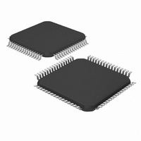
IC MCU/DSP 32KB FLASH 64TQFP
Manufacturer
Microchip Technology
Series
dsPIC™ 33Fr
Specifications of DSPIC33FJ32GS406-I/PT
Core Processor
dsPIC
Core Size
16-Bit
Speed
40 MIPs
Connectivity
I²C, IrDA, LIN, SCI, SPI, UART/USART, USB
Peripherals
Brown-out Detect/Reset, QEI, POR, PWM, WDT
Number Of I /o
58
Program Memory Size
32KB (32K x 8)
Program Memory Type
FLASH
Ram Size
4K x 8
Voltage - Supply (vcc/vdd)
3 V ~ 3.6 V
Data Converters
A/D 16x10b
Oscillator Type
Internal
Operating Temperature
-40°C ~ 85°C
Package / Case
64-TFQFP
Core Frequency
40MHz
Embedded Interface Type
I2C, SPI, UART
No. Of I/o's
53
Flash Memory Size
32KB
Supply Voltage Range
3V To 3.6V
Rohs Compliant
Yes
Lead Free Status / RoHS Status
Lead free / RoHS Compliant
Eeprom Size
-
Lead Free Status / RoHS Status
Lead free / RoHS Compliant, Lead free / RoHS Compliant
Available stocks
Company
Part Number
Manufacturer
Quantity
Price
Company:

Part Number:
DSPIC33FJ32GS406-I/PT
Manufacturer:
Microchip Technology
Quantity:
10 000


dsPIC33FJ32GS406/606/608/610 and dsPIC33FJ64GS406/606/608/610
REGISTER 17-2:
DS70591C-page 258
bit 15
bit 7
Legend:
R = Readable bit
-n = Value at POR
bit 15-11
bit 10-9
bit 8
bit 7
bit 6-4
bit 3-0
QEOUT
R/W-0
U-0
—
Unimplemented: Read as ‘0’
IMV<1:0>: Index Match Value bits – These bits allow the user application to specify the state of the
QEAx and QEBx input pins during an Index pulse when the POSxCNT register is to be reset.
In x4 Quadrature Count Mode:
In x4 Quadrature Count Mode:
CEID: Count Error Interrupt Disable bit
1 = Interrupts due to count errors are disabled
0 = Interrupts due to count errors are enabled
QEOUT: QEAx/QEBx/INDXx Pin Digital Filter Output Enable bit
1 = Digital filter outputs enabled
0 = Digital filter outputs disabled (normal pin operation)
QECK<2:0>: QEAx/QEBx/INDXx Digital Filter Clock Divide Select Bits
111 = 1:256 Clock Divide
110 = 1:128 Clock Divide
101 = 1:64 Clock Divide
100 = 1:32 Clock Divide
011 = 1:16 Clock Divide
010 = 1:4 Clock Divide
001 = 1:2 Clock Divide
000 = 1:1 Clock Divide
Unimplemented: Read as ‘0’
IMV1 = Required State of Phase B input signal for match on index pulse
IMV0 = Required State of Phase A input signal for match on index pulse
IMV1 = Selects Phase input signal for Index state match (0 = Phase A, 1 = Phase B)
IMV0 = Required state of the selected Phase input signal for match on index pulse
U-0
—
DFLTxCON: DIGITAL FILTER CONTROL REGISTER
W = Writable bit
QECK<2:0>
‘1’ = Bit is set
R/W-0
U-0
—
U-0
Preliminary
—
U = Unimplemented bit, read as ‘0’
‘0’ = Bit is cleared
U-0
U-0
—
—
R/W-0
U-0
—
IMV<2:0>
2010 Microchip Technology Inc.
x = Bit is unknown
R/W-0
U-0
—
R/W-0
CEID
U-0
—
bit 8
bit 0
Related parts for DSPIC33FJ32GS406-I/PT
Image
Part Number
Description
Manufacturer
Datasheet
Request
R

Part Number:
Description:
IC, DSC, 16BIT, 12KB, 40MHZ, 3.6V, DIP28
Manufacturer:
Microchip Technology
Datasheet:

Part Number:
Description:
Manufacturer:
Microchip Technology Inc.
Datasheet:
Part Number:
Description:
Manufacturer:
Microchip Technology Inc.
Datasheet:
Part Number:
Description:
Manufacturer:
Microchip Technology Inc.
Datasheet:
Part Number:
Description:
Manufacturer:
Microchip Technology Inc.
Datasheet:
Part Number:
Description:
Manufacturer:
Microchip Technology Inc.
Datasheet:
Part Number:
Description:
Manufacturer:
Microchip Technology Inc.
Datasheet:
Part Number:
Description:
Manufacturer:
Microchip Technology Inc.
Datasheet:
Part Number:
Description:
Manufacturer:
Microchip Technology Inc.
Datasheet: