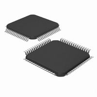
DSPIC33FJ32GS406-I/PT Microchip Technology, DSPIC33FJ32GS406-I/PT Datasheet - Page 23

DSPIC33FJ32GS406-I/PT
Manufacturer Part Number
DSPIC33FJ32GS406-I/PT
Description
IC MCU/DSP 32KB FLASH 64TQFP
Manufacturer
Microchip Technology
Series
dsPIC™ 33Fr
Specifications of DSPIC33FJ32GS406-I/PT
Core Processor
dsPIC
Core Size
16-Bit
Speed
40 MIPs
Connectivity
I²C, IrDA, LIN, SCI, SPI, UART/USART, USB
Peripherals
Brown-out Detect/Reset, QEI, POR, PWM, WDT
Number Of I /o
58
Program Memory Size
32KB (32K x 8)
Program Memory Type
FLASH
Ram Size
4K x 8
Voltage - Supply (vcc/vdd)
3 V ~ 3.6 V
Data Converters
A/D 16x10b
Oscillator Type
Internal
Operating Temperature
-40°C ~ 85°C
Package / Case
64-TFQFP
Core Frequency
40MHz
Embedded Interface Type
I2C, SPI, UART
No. Of I/o's
53
Flash Memory Size
32KB
Supply Voltage Range
3V To 3.6V
Rohs Compliant
Yes
Lead Free Status / RoHS Status
Lead free / RoHS Compliant
Eeprom Size
-
Lead Free Status / RoHS Status
Lead free / RoHS Compliant, Lead free / RoHS Compliant
Available stocks
Company
Part Number
Manufacturer
Quantity
Price
Company:
Part Number:
DSPIC33FJ32GS406-I/PT
Manufacturer:
Microchip Technology
Quantity:
10 000
- Current page: 23 of 418
- Download datasheet (3Mb)
TABLE 1-1:
2010 Microchip Technology Inc.
FLT1-FLT23
SYNCI1-SYNCI4
SYNCO1-SYNCO2
PWM1L
PWM1H
PWM2L
PWM2H
PWM3L
PWM3H
PWM4L
PWM4H
PWM5L
PWM5H
PWM6L
PWM6H
PWM7L
PWM7H
PWM8L
PWM8H
PWM9L
PWM9H
PGED1
PGEC1
PGED2
PGEC2
PGED3
PGEC3
MCLR
AV
AV
V
V
V
Legend: CMOS = CMOS compatible input or output
DD
CAP
SS
dsPIC33FJ32GS406/606/608/610 and dsPIC33FJ64GS406/606/608/610
DD
SS
/V
Pin Name
DDCORE
ST = Schmitt Trigger input with CMOS levels
TTL = Transistor-Transistor Logic
PINOUT I/O DESCRIPTIONS (CONTINUED)
Type
Pin
I/O
I/O
I/O
I/P
O
O
O
O
O
O
O
O
O
O
O
O
O
O
O
O
O
O
O
P
P
P
P
P
I
I
I
I
I
Buffer
Type
ST
ST
ST
ST
ST
ST
ST
ST
ST
—
—
—
—
—
—
—
—
—
—
—
—
—
—
—
—
—
—
—
—
—
—
P
P
Fault Inputs to PWM Module
External synchronization signal to PWM Master Time Base
PWM Master Time Base for external device synchronization
PWM1 Low output
PWM1 High output
PWM2 Low output
PWM2 High output
PWM3 Low output
PWM3 High output
PWM4 Low output
PWM4 High output
PWM5 Low output
PWM5 High output
PWM6 Low output
PWM6 High output
PWM7 Low output
PWM7 High output
PWM8 Low output
PWM8 High output
PWM9 Low output
PWM9 High output
Data I/O pin for programming/debugging communication Channel 1
Clock input pin for programming/debugging communication Channel 1
Data I/O pin for programming/debugging communication Channel 2
Clock input pin for programming/debugging communication Channel 2
Data I/O pin for programming/debugging communication Channel 3
Clock input pin for programming/debugging communication Channel 3
Master Clear (Reset) input. This pin is an active-low Reset to the
device.
Positive supply for analog modules
Ground reference for analog modules
Positive supply for peripheral logic and I/O pins
CPU logic filter capacitor connection
Ground reference for logic and I/O pins
Preliminary
Analog = Analog input
P = Power
Description
I = Input
O = Output
DS70591C-page 23
Related parts for DSPIC33FJ32GS406-I/PT
Image
Part Number
Description
Manufacturer
Datasheet
Request
R

Part Number:
Description:
IC, DSC, 16BIT, 12KB, 40MHZ, 3.6V, DIP28
Manufacturer:
Microchip Technology
Datasheet:

Part Number:
Description:
Manufacturer:
Microchip Technology Inc.
Datasheet:

Part Number:
Description:
Manufacturer:
Microchip Technology Inc.
Datasheet:

Part Number:
Description:
Manufacturer:
Microchip Technology Inc.
Datasheet:

Part Number:
Description:
Manufacturer:
Microchip Technology Inc.
Datasheet:

Part Number:
Description:
Manufacturer:
Microchip Technology Inc.
Datasheet:

Part Number:
Description:
Manufacturer:
Microchip Technology Inc.
Datasheet:

Part Number:
Description:
Manufacturer:
Microchip Technology Inc.
Datasheet:

Part Number:
Description:
Manufacturer:
Microchip Technology Inc.
Datasheet:


