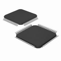
DSPIC33FJ32GS406-I/PT Microchip Technology, DSPIC33FJ32GS406-I/PT Datasheet - Page 314

DSPIC33FJ32GS406-I/PT
Manufacturer Part Number
DSPIC33FJ32GS406-I/PT
Description
IC MCU/DSP 32KB FLASH 64TQFP
Manufacturer
Microchip Technology
Series
dsPIC™ 33Fr
Specifications of DSPIC33FJ32GS406-I/PT
Core Processor
dsPIC
Core Size
16-Bit
Speed
40 MIPs
Connectivity
I²C, IrDA, LIN, SCI, SPI, UART/USART, USB
Peripherals
Brown-out Detect/Reset, QEI, POR, PWM, WDT
Number Of I /o
58
Program Memory Size
32KB (32K x 8)
Program Memory Type
FLASH
Ram Size
4K x 8
Voltage - Supply (vcc/vdd)
3 V ~ 3.6 V
Data Converters
A/D 16x10b
Oscillator Type
Internal
Operating Temperature
-40°C ~ 85°C
Package / Case
64-TFQFP
Core Frequency
40MHz
Embedded Interface Type
I2C, SPI, UART
No. Of I/o's
53
Flash Memory Size
32KB
Supply Voltage Range
3V To 3.6V
Rohs Compliant
Yes
Lead Free Status / RoHS Status
Lead free / RoHS Compliant
Eeprom Size
-
Lead Free Status / RoHS Status
Lead free / RoHS Compliant, Lead free / RoHS Compliant
Available stocks
Company
Part Number
Manufacturer
Quantity
Price
Company:
Part Number:
DSPIC33FJ32GS406-I/PT
Manufacturer:
Microchip Technology
Quantity:
10 000
- Current page: 314 of 418
- Download datasheet (3Mb)
dsPIC33FJ32GS406/606/608/610 and dsPIC33FJ64GS406/606/608/610
REGISTER 22-3:
DS70591C-page 314
bit 15
bit 7
Legend:
R = Readable bit
-n = Value at POR
bit 15-1
bit 0
Note 1: The encoding results are shifted left two bits so bits 1-0 of the result are always zero.
R/W-0
R/W-0
2: As an alternative to using the ADBASE Register, the ADCP0-ADCP12 ADC Pair Conversion Complete
Interrupts can be used to invoke A to D conversion completion routines for individual ADC input pairs.
ADBASE<15:1>: This register contains the base address of the user’s ADC Interrupt Service Routine
jump table. This register, when read, contains the sum of the ADBASE register contents and the
encoded value of the PxRDY Status bits.
The encoder logic provides the bit number of the highest priority PxRDY bits where P0RDY is the
highest priority, and P6RDY is the lowest priority.
Unimplemented: Read as ‘0’
R/W-0
R/W-0
ADBASE: A/D BASE REGISTER
W = Writable bit
‘1’ = Bit is set
R/W-0
R/W-0
ADBASE<7:1>
R/W-0
R/W-0
Preliminary
ADBASE<15:8>
U = Unimplemented bit, read as ‘0’
‘0’ = Bit is cleared
(1,2)
R/W-0
R/W-0
R/W-0
R/W-0
2010 Microchip Technology Inc.
x = Bit is unknown
R/W-0
R/W-0
R/W-0
U-0
—
bit 8
bit 0
Related parts for DSPIC33FJ32GS406-I/PT
Image
Part Number
Description
Manufacturer
Datasheet
Request
R

Part Number:
Description:
IC, DSC, 16BIT, 12KB, 40MHZ, 3.6V, DIP28
Manufacturer:
Microchip Technology
Datasheet:

Part Number:
Description:
Manufacturer:
Microchip Technology Inc.
Datasheet:

Part Number:
Description:
Manufacturer:
Microchip Technology Inc.
Datasheet:

Part Number:
Description:
Manufacturer:
Microchip Technology Inc.
Datasheet:

Part Number:
Description:
Manufacturer:
Microchip Technology Inc.
Datasheet:

Part Number:
Description:
Manufacturer:
Microchip Technology Inc.
Datasheet:

Part Number:
Description:
Manufacturer:
Microchip Technology Inc.
Datasheet:

Part Number:
Description:
Manufacturer:
Microchip Technology Inc.
Datasheet:

Part Number:
Description:
Manufacturer:
Microchip Technology Inc.
Datasheet:


