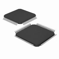
DSPIC33FJ32GS406-I/PT Microchip Technology, DSPIC33FJ32GS406-I/PT Datasheet - Page 335

DSPIC33FJ32GS406-I/PT
Manufacturer Part Number
DSPIC33FJ32GS406-I/PT
Description
IC MCU/DSP 32KB FLASH 64TQFP
Manufacturer
Microchip Technology
Series
dsPIC™ 33Fr
Specifications of DSPIC33FJ32GS406-I/PT
Core Processor
dsPIC
Core Size
16-Bit
Speed
40 MIPs
Connectivity
I²C, IrDA, LIN, SCI, SPI, UART/USART, USB
Peripherals
Brown-out Detect/Reset, QEI, POR, PWM, WDT
Number Of I /o
58
Program Memory Size
32KB (32K x 8)
Program Memory Type
FLASH
Ram Size
4K x 8
Voltage - Supply (vcc/vdd)
3 V ~ 3.6 V
Data Converters
A/D 16x10b
Oscillator Type
Internal
Operating Temperature
-40°C ~ 85°C
Package / Case
64-TFQFP
Core Frequency
40MHz
Embedded Interface Type
I2C, SPI, UART
No. Of I/o's
53
Flash Memory Size
32KB
Supply Voltage Range
3V To 3.6V
Rohs Compliant
Yes
Lead Free Status / RoHS Status
Lead free / RoHS Compliant
Eeprom Size
-
Lead Free Status / RoHS Status
Lead free / RoHS Compliant, Lead free / RoHS Compliant
Available stocks
Company
Part Number
Manufacturer
Quantity
Price
Company:
Part Number:
DSPIC33FJ32GS406-I/PT
Manufacturer:
Microchip Technology
Quantity:
10 000
- Current page: 335 of 418
- Download datasheet (3Mb)
TABLE 24-2:
2010 Microchip Technology Inc.
FWDTEN
WINDIS
WDTPRE
WDTPOST<3:0>
FPWRT<2:0>
JTAGEN
ICS<1:0>
ALTQIO
ALTSS1
CMPPOL0
HYST0<1:0>
dsPIC33FJ32GS406/606/608/610 and dsPIC33FJ64GS406/606/608/610
Bit Field
dsPIC33F CONFIGURATION BITS DESCRIPTION (CONTINUED)
Register
FWDT
FWDT
FWDT
FWDT
FCMP
FPOR
FPOR
FPOR
FCMP
FICD
FICD
Watchdog Timer Enable bit
1 = Watchdog Timer always enabled (LPRC oscillator cannot be disabled;
0 = Watchdog Timer enabled/disabled by user software (LPRC can be
Watchdog Timer Window Enable bit
1 = Watchdog Timer in Non-Window mode
0 = Watchdog Timer in Window mode
Watchdog Timer Prescaler bit
1 = 1:128
0 = 1:32
Watchdog Timer Postscaler bits
1111 = 1:32,768
1110 = 1:16,384
•
•
•
0001 = 1:2
0000 = 1:1
Power-on Reset Timer Value Select bits
111 = PWRT = 128 ms
110 = PWRT = 64 ms
101 = PWRT = 32 ms
100 = PWRT = 16 ms
011 = PWRT = 8 ms
010 = PWRT = 4 ms
001 = PWRT = 2 ms
000 = PWRT = Disabled
JTAG Enable bit
1 = JTAG is enabled
0 = JTAG is disabled
11 = Communicate on PGEC1 and PGED1
10 = Communicate on PGEC2 and PGED2
01 = Communicate on PGEC3 and PGED3
00 = Reserved, do not use.
Enable Alternate QEI1 pin bit
1 = QEA1, QEB1 and INDX1 are selected as inputs to QEI1
0 = AQEA1, AQEB1 and AINDX1 are selected as inputs to QEI1
1 = ASS1 is selected as the I/O pin for SPI1
0 = SS1 is selected as the I/O pin for SPI1
Comparator Hysteresis Polarity (for even numbered comparators)
1 = Hysteresis is applied to falling edge
0 = Hysteresis is applied to rising edge
Comparator Hysteresis Select
11 = 45 mV Hysteresis
10 = 30 mV Hysteresis
01 = 15 mV Hysteresis
00 = No Hysteresis
ICD Communication Channel Select Enable bits
Enable Alternate SS1 pin bit
clearing the SWDTEN bit in the RCON register will have no effect)
disabled by clearing the SWDTEN bit in the RCON register)
Preliminary
Description
DS70591C-page 335
Related parts for DSPIC33FJ32GS406-I/PT
Image
Part Number
Description
Manufacturer
Datasheet
Request
R

Part Number:
Description:
IC, DSC, 16BIT, 12KB, 40MHZ, 3.6V, DIP28
Manufacturer:
Microchip Technology
Datasheet:

Part Number:
Description:
Manufacturer:
Microchip Technology Inc.
Datasheet:

Part Number:
Description:
Manufacturer:
Microchip Technology Inc.
Datasheet:

Part Number:
Description:
Manufacturer:
Microchip Technology Inc.
Datasheet:

Part Number:
Description:
Manufacturer:
Microchip Technology Inc.
Datasheet:

Part Number:
Description:
Manufacturer:
Microchip Technology Inc.
Datasheet:

Part Number:
Description:
Manufacturer:
Microchip Technology Inc.
Datasheet:

Part Number:
Description:
Manufacturer:
Microchip Technology Inc.
Datasheet:

Part Number:
Description:
Manufacturer:
Microchip Technology Inc.
Datasheet:


