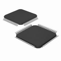
DSPIC33FJ32GS406-I/PT Microchip Technology, DSPIC33FJ32GS406-I/PT Datasheet - Page 306

DSPIC33FJ32GS406-I/PT
Manufacturer Part Number
DSPIC33FJ32GS406-I/PT
Description
IC MCU/DSP 32KB FLASH 64TQFP
Manufacturer
Microchip Technology
Series
dsPIC™ 33Fr
Specifications of DSPIC33FJ32GS406-I/PT
Core Processor
dsPIC
Core Size
16-Bit
Speed
40 MIPs
Connectivity
I²C, IrDA, LIN, SCI, SPI, UART/USART, USB
Peripherals
Brown-out Detect/Reset, QEI, POR, PWM, WDT
Number Of I /o
58
Program Memory Size
32KB (32K x 8)
Program Memory Type
FLASH
Ram Size
4K x 8
Voltage - Supply (vcc/vdd)
3 V ~ 3.6 V
Data Converters
A/D 16x10b
Oscillator Type
Internal
Operating Temperature
-40°C ~ 85°C
Package / Case
64-TFQFP
Core Frequency
40MHz
Embedded Interface Type
I2C, SPI, UART
No. Of I/o's
53
Flash Memory Size
32KB
Supply Voltage Range
3V To 3.6V
Rohs Compliant
Yes
Lead Free Status / RoHS Status
Lead free / RoHS Compliant
Eeprom Size
-
Lead Free Status / RoHS Status
Lead free / RoHS Compliant, Lead free / RoHS Compliant
Available stocks
Company
Part Number
Manufacturer
Quantity
Price
Company:
Part Number:
DSPIC33FJ32GS406-I/PT
Manufacturer:
Microchip Technology
Quantity:
10 000
- Current page: 306 of 418
- Download datasheet (3Mb)
dsPIC33FJ32GS406/606/608/610 and dsPIC33FJ64GS406/606/608/610
22.3
The high-speed 10-bit ADC is designed to support
power conversion applications when used with the
High-Speed PWM module. The ADC may have one or
two SAR modules, depending on the device variant. If
two SARs are present on a device, two conversions
can be processed at a time, yielding 4 Msps conversion
rate. If only one SAR is present on a device, only one
conversion can be processed at a time, yielding 2 Msps
conversion rate. The high-speed 10-bit ADC produces
two 10-bit conversion results in a 0.5 microsecond.
The ADC module supports up to 24 external analog
inputs and two internal analog inputs. To monitor
reference voltage, two internal inputs, AN24 and AN25,
are connected to the EXTREF and internal band gap
voltages (1.2V), respectively.
The analog reference voltage is defined as the device
supply voltage (AV
DS70591C-page 306
Module Functionality
DD
/AV
SS
).
Preliminary
The ADC module uses the following control and
STATUS registers:
• ADCON: A/D Control Register
• ADSTAT: A/D Status Register
• ADBASE: A/D Base Register
• ADPCFG: A/D Port Configuration Register
• ADPCFG2: A/D Port Configuration Register 2
• ADCPC0: A/D Convert Pair Control Register 0
• ADCPC1: A/D Convert Pair Control Register 1
• ADCPC2: A/D Convert Pair Control Register 2
• ADCPC3: A/D Convert Pair Control Register 3
• ADCPC4: A/D Convert Pair Control Register 4
• ADCPC5: A/D Convert Pair Control Register 5
• ADCPC6: A/D Convert Pair Control Register 6
The ADCON register controls the operation of the
ADC module. The ADSTAT register displays the
status of the conversion processes. The ADPCFG
registers configure the port pins as analog inputs or
as digital I/O. The ADCPCx registers control the
triggering of the ADC conversions. See Register 22-1
through Register 22-12 for detailed bit configurations.
Note:
A unique feature of the ADC module is its
ability
asynchronous manner. Individual sample
and hold circuits can be triggered
independently of each other.
to
2010 Microchip Technology Inc.
sample
inputs
in
an
Related parts for DSPIC33FJ32GS406-I/PT
Image
Part Number
Description
Manufacturer
Datasheet
Request
R

Part Number:
Description:
IC, DSC, 16BIT, 12KB, 40MHZ, 3.6V, DIP28
Manufacturer:
Microchip Technology
Datasheet:

Part Number:
Description:
Manufacturer:
Microchip Technology Inc.
Datasheet:

Part Number:
Description:
Manufacturer:
Microchip Technology Inc.
Datasheet:

Part Number:
Description:
Manufacturer:
Microchip Technology Inc.
Datasheet:

Part Number:
Description:
Manufacturer:
Microchip Technology Inc.
Datasheet:

Part Number:
Description:
Manufacturer:
Microchip Technology Inc.
Datasheet:

Part Number:
Description:
Manufacturer:
Microchip Technology Inc.
Datasheet:

Part Number:
Description:
Manufacturer:
Microchip Technology Inc.
Datasheet:

Part Number:
Description:
Manufacturer:
Microchip Technology Inc.
Datasheet:


