TOOLSTICK540DC Silicon Laboratories Inc, TOOLSTICK540DC Datasheet - Page 7
TOOLSTICK540DC
Manufacturer Part Number
TOOLSTICK540DC
Description
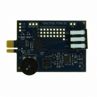
DAUGHTER CARD TOOLSTICK F540
Manufacturer
Silicon Laboratories Inc
Series
ToolStickr
Type
MCUr
Datasheets
1.TOOLSTICK540DC.pdf
(274 pages)
2.TOOLSTICK540DC.pdf
(16 pages)
3.TOOLSTICK540DC.pdf
(12 pages)
Specifications of TOOLSTICK540DC
Contents
Daughter Card
Processor To Be Evaluated
C8051F54x
Processor Series
C8051F54x
Interface Type
USB
Operating Supply Voltage
2.7 V to 3.6 V
Lead Free Status / RoHS Status
Lead free / RoHS Compliant
For Use With/related Products
C8051F54x
For Use With
336-1345 - TOOLSTICK BASE ADAPTER336-1182 - ADAPTER USB DEBUG FOR C8051FXXX
Lead Free Status / Rohs Status
Lead free / RoHS Compliant
Other names
336-1717


C8051F54x
Figure 17.3. External 32.768 kHz Quartz Crystal Oscillator Connection Diagram 145
Figure 18.1. Port I/O Functional Block Diagram .................................................... 147
Figure 18.2. Port I/O Cell Block Diagram .............................................................. 148
Figure 18.3. Peripheral Availability on Port I/O Pins .............................................. 151
Figure 18.4. Crossbar Priority Decoder in Example Configuration ........................ 152
Figure 19.1. LIN Block Diagram ............................................................................ 170
Figure 20.1. SMBus Block Diagram ...................................................................... 187
Figure 20.2. Typical SMBus Configuration ............................................................ 188
Figure 20.3. SMBus Transaction ........................................................................... 189
Figure 20.4. Typical SMBus SCL Generation ........................................................ 191
Figure 20.5. Typical Master Write Sequence ........................................................ 198
Figure 20.6. Typical Master Read Sequence ........................................................ 199
Figure 20.7. Typical Slave Write Sequence .......................................................... 200
Figure 20.8. Typical Slave Read Sequence .......................................................... 201
Figure 21.1. UART0 Block Diagram ...................................................................... 205
Figure 21.2. UART0 Timing Without Parity or Extra Bit ......................................... 207
Figure 21.3. UART0 Timing With Parity ................................................................ 207
Figure 21.4. UART0 Timing With Extra Bit ............................................................ 207
Figure 21.5. Typical UART Interconnect Diagram ................................................. 208
Figure 21.6. UART Multi-Processor Mode Interconnect Diagram ......................... 209
Figure 22.1. SPI Block Diagram ............................................................................ 214
Figure 22.2. Multiple-Master Mode Connection Diagram ...................................... 217
Figure 22.3. 3-Wire Single Master and 3-Wire Single Slave Mode Connection Diagram
217
Figure 22.4. 4-Wire Single Master Mode and 4-Wire Slave Mode Connection Diagram
217
Figure 22.5. Master Mode Data/Clock Timing ....................................................... 219
Figure 22.6. Slave Mode Data/Clock Timing (CKPHA = 0) ................................... 220
Figure 22.7. Slave Mode Data/Clock Timing (CKPHA = 1) ................................... 220
Figure 22.8. SPI Master Timing (CKPHA = 0) ....................................................... 224
Figure 22.9. SPI Master Timing (CKPHA = 1) ....................................................... 224
Figure 22.10. SPI Slave Timing (CKPHA = 0) ....................................................... 225
Figure 22.11. SPI Slave Timing (CKPHA = 1) ....................................................... 225
Figure 23.1. T0 Mode 0 Block Diagram ................................................................. 230
Figure 23.2. T0 Mode 2 Block Diagram ................................................................. 231
Figure 23.3. T0 Mode 3 Block Diagram ................................................................. 232
Figure 23.4. Timer 2 16-Bit Mode Block Diagram ................................................. 237
Figure 23.5. Timer 2 8-Bit Mode Block Diagram ................................................... 238
Figure 23.6. Timer 2 External Oscillator Capture Mode Block Diagram ................ 239
Figure 23.7. Timer 3 16-Bit Mode Block Diagram ................................................. 243
Figure 23.8. Timer 3 8-Bit Mode Block Diagram ................................................... 244
Figure 23.9. Timer 3 External Oscillator Capture Mode Block Diagram ................ 245
Figure 24.1. PCA Block Diagram ........................................................................... 249
Figure 24.2. PCA Counter/Timer Block Diagram ................................................... 251
Rev. 1.1
7
Related parts for TOOLSTICK540DC
Image
Part Number
Description
Manufacturer
Datasheet
Request
R

Part Number:
Description:
KIT TOOL EVAL SYS IN A USB STICK
Manufacturer:
Silicon Laboratories Inc
Datasheet:

Part Number:
Description:
TOOLSTICK DEBUG ADAPTER
Manufacturer:
Silicon Laboratories Inc
Datasheet:

Part Number:
Description:
TOOLSTICK BASE ADAPTER
Manufacturer:
Silicon Laboratories Inc
Datasheet:

Part Number:
Description:
TOOLSTICK DAUGHTER CARD
Manufacturer:
Silicon Laboratories Inc
Datasheet:

Part Number:
Description:
TOOLSTICK DAUGHTER CARD
Manufacturer:
Silicon Laboratories Inc
Datasheet:

Part Number:
Description:
TOOLSTICK DAUGHTER CARD
Manufacturer:
Silicon Laboratories Inc
Datasheet:

Part Number:
Description:
TOOLSTICK PROGRAMMING ADAPTER
Manufacturer:
Silicon Laboratories Inc
Datasheet:

Part Number:
Description:
TOOLSTICK DAUGHTER CARD
Manufacturer:
Silicon Laboratories Inc
Datasheet:

Part Number:
Description:
KIT STARTER TOOLSTICK
Manufacturer:
Silicon Laboratories Inc
Datasheet:

Part Number:
Description:
KIT UNIVERSITY TOOLSTICK STARTER
Manufacturer:
Silicon Laboratories Inc
Datasheet:

Part Number:
Description:
DAUGHTER CARD TOOLSTICK F330
Manufacturer:
Silicon Laboratories Inc
Datasheet:

Part Number:
Description:
CARD DAUGHTER UNIVRSTY TOOLSTICK
Manufacturer:
Silicon Laboratories Inc
Datasheet:

Part Number:
Description:
DAUGHTER CARD TOOLSTICK F582
Manufacturer:
Silicon Laboratories Inc
Datasheet:

Part Number:
Description:
DAUGHTER CARD TOOLSTICK F500
Manufacturer:
Silicon Laboratories Inc
Datasheet:

Part Number:
Description:
DAUGHTER CARD TOOLSTICK F560
Manufacturer:
Silicon Laboratories Inc
Datasheet: