TOOLSTICK540DC Silicon Laboratories Inc, TOOLSTICK540DC Datasheet - Page 151
TOOLSTICK540DC
Manufacturer Part Number
TOOLSTICK540DC
Description
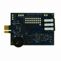
DAUGHTER CARD TOOLSTICK F540
Manufacturer
Silicon Laboratories Inc
Series
ToolStickr
Type
MCUr
Datasheets
1.TOOLSTICK540DC.pdf
(274 pages)
2.TOOLSTICK540DC.pdf
(16 pages)
3.TOOLSTICK540DC.pdf
(12 pages)
Specifications of TOOLSTICK540DC
Contents
Daughter Card
Processor To Be Evaluated
C8051F54x
Processor Series
C8051F54x
Interface Type
USB
Operating Supply Voltage
2.7 V to 3.6 V
Lead Free Status / RoHS Status
Lead free / RoHS Compliant
For Use With/related Products
C8051F54x
For Use With
336-1345 - TOOLSTICK BASE ADAPTER336-1182 - ADAPTER USB DEBUG FOR C8051FXXX
Lead Free Status / Rohs Status
Lead free / RoHS Compliant
Other names
336-1717


Registers XBR0, XBR1, and XBR2 are used to assign the digital I/O resources to the physical I/O Port
pins. Note that when the SMBus is selected, the Crossbar assigns both pins associated with the SMBus
(SDA and SCL); and similarly when the UART or LIN are selected, the Crossbar assigns both pins associ-
ated with the peripheral (TX and RX). UART0 pin assignments are fixed for bootloading purposes: UART
TX0 is always assigned to P0.4; UART RX0 is always assigned to P0.5. Standard Port I/Os appear contig-
uously after the prioritized functions have been assigned.
Important Note: The SPI can be operated in either 3-wire or 4-wire modes, pending the state of the
NSSMD1–NSSMD0 bits in register SPI0CN. According to the SPI mode, the NSS signal may or may not
be routed to a Port pin.
As an example configuration, if SPI0 in 4-wire mode, and PCA0 Modules 0, 1, and 2 are enabled on the
crossbar with P0.1, P0.2, and P0.5 skipped, the registers should be set as follows: XBR0 = 0x04 (SPI0
enabled), XBR1 = 0x0C (PCA0 modules 0, 1, and 2 enabled), XBR2 = 0x40 (Crossbar enabled), and
P0SKIP = 0x26 (P0.1, P0.2, and P0.5 skipped). The resulting crossbar would look as shown in
Figure 18.4.
Port
Special
Function
Signals
PIN I/O
UART_TX
UART_RX
SCK
MISO
MOSI
NSS
SDA
SCL
CP0
CP0A
CP1
CP1A
SYSCLK
CEX0
CEX1
CEX2
CEX3
CEX4
CEX5
ECI
T0
T1
LIN_TX
LIN_RX
0 1 2 3
Figure 18.3. Peripheral Availability on Port I/O Pins
P0
4 5 6
7 0 1 2
Rev. 1.1
3 4 5 6
P1
7 0 1 2
available on the 32-pin
P2.2-P2.7, P3.0 only
3 4 5 6
P2
packages
C8051F54x
7 0
P3
151
Related parts for TOOLSTICK540DC
Image
Part Number
Description
Manufacturer
Datasheet
Request
R

Part Number:
Description:
KIT TOOL EVAL SYS IN A USB STICK
Manufacturer:
Silicon Laboratories Inc
Datasheet:

Part Number:
Description:
TOOLSTICK DEBUG ADAPTER
Manufacturer:
Silicon Laboratories Inc
Datasheet:

Part Number:
Description:
TOOLSTICK BASE ADAPTER
Manufacturer:
Silicon Laboratories Inc
Datasheet:

Part Number:
Description:
TOOLSTICK DAUGHTER CARD
Manufacturer:
Silicon Laboratories Inc
Datasheet:

Part Number:
Description:
TOOLSTICK DAUGHTER CARD
Manufacturer:
Silicon Laboratories Inc
Datasheet:

Part Number:
Description:
TOOLSTICK DAUGHTER CARD
Manufacturer:
Silicon Laboratories Inc
Datasheet:

Part Number:
Description:
TOOLSTICK PROGRAMMING ADAPTER
Manufacturer:
Silicon Laboratories Inc
Datasheet:

Part Number:
Description:
TOOLSTICK DAUGHTER CARD
Manufacturer:
Silicon Laboratories Inc
Datasheet:

Part Number:
Description:
KIT STARTER TOOLSTICK
Manufacturer:
Silicon Laboratories Inc
Datasheet:

Part Number:
Description:
KIT UNIVERSITY TOOLSTICK STARTER
Manufacturer:
Silicon Laboratories Inc
Datasheet:

Part Number:
Description:
DAUGHTER CARD TOOLSTICK F330
Manufacturer:
Silicon Laboratories Inc
Datasheet:

Part Number:
Description:
CARD DAUGHTER UNIVRSTY TOOLSTICK
Manufacturer:
Silicon Laboratories Inc
Datasheet:

Part Number:
Description:
DAUGHTER CARD TOOLSTICK F582
Manufacturer:
Silicon Laboratories Inc
Datasheet:

Part Number:
Description:
DAUGHTER CARD TOOLSTICK F500
Manufacturer:
Silicon Laboratories Inc
Datasheet:

Part Number:
Description:
DAUGHTER CARD TOOLSTICK F560
Manufacturer:
Silicon Laboratories Inc
Datasheet: