TOOLSTICK540DC Silicon Laboratories Inc, TOOLSTICK540DC Datasheet - Page 132
TOOLSTICK540DC
Manufacturer Part Number
TOOLSTICK540DC
Description
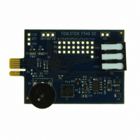
DAUGHTER CARD TOOLSTICK F540
Manufacturer
Silicon Laboratories Inc
Series
ToolStickr
Type
MCUr
Datasheets
1.TOOLSTICK540DC.pdf
(274 pages)
2.TOOLSTICK540DC.pdf
(16 pages)
3.TOOLSTICK540DC.pdf
(12 pages)
Specifications of TOOLSTICK540DC
Contents
Daughter Card
Processor To Be Evaluated
C8051F54x
Processor Series
C8051F54x
Interface Type
USB
Operating Supply Voltage
2.7 V to 3.6 V
Lead Free Status / RoHS Status
Lead free / RoHS Compliant
For Use With/related Products
C8051F54x
For Use With
336-1345 - TOOLSTICK BASE ADAPTER336-1182 - ADAPTER USB DEBUG FOR C8051FXXX
Lead Free Status / Rohs Status
Lead free / RoHS Compliant
Other names
336-1717


C8051F54x
SFR Definition 16.1. VDM0CN: V
SFR Address = 0xFF; SFR Page = 0x00
16.3. External Reset
The external RST pin provides a means for external circuitry to force the device into a reset state. Assert-
ing an active-low signal on the RST pin generates a reset; an external pullup and/or decoupling of the RST
pin may be necessary to avoid erroneous noise-induced resets. See Table 6.4 for complete RST pin spec-
ifications. The PINRSF flag (RSTSRC.0) is set on exit from an external reset.
16.4. Missing Clock Detector Reset
The Missing Clock Detector (MCD) is a one-shot circuit that is triggered by the system clock. If the system
clock remains high or low for more than the time specified in Table 6.4, “Reset Electrical Characteristics,”
on page 52, the one-shot will time out and generate a reset. After a MCD reset, the MCDRSF flag (RST-
SRC.2) will read 1, signifying the MCD as the reset source; otherwise, this bit reads 0. Writing a 1 to the
MCDRSF bit enables the Missing Clock Detector; writing a 0 disables it. The state of the RST pin is unaf-
fected by this reset.
132
Name
Reset
4:0
Bit
Type
7
6
5
Bit
VDDSTAT
VDMLVL
VDMEN
Unused
VDMEN
Name
Varies
R/W
7
VDDSTAT
V
This bit turns the V
tem resets until it is also selected as a reset source in register RSTSRC (SFR Def-
inition 16.2). Selecting the V
may generate a system reset. In systems where this reset would be undesirable, a
delay should be introduced between enabling the V
reset source. See Table 6.4 for the minimum V
0: V
1: V
V
This bit indicates the current power supply status (V
0: V
1: V
V
0: V
1: V
tem includes code that writes to and/or erases Flash.
Read = 00000b; Write = Don’t care.
Varies
DD
DD
DD
R
6
DD
DD
DD
DD
DD
DD
Monitor Enable.
Status.
Monitor Level Select.
Monitor Disabled.
Monitor Enabled.
is at or below the V
is above the V
Monitor Threshold is set to VRST-LOW
Monitor Threshold is set to VRST-HIGH. This setting is required for any sys-
VDMLVL
R/W
5
0
DD
DD
DD
monitor circuit on/off. The V
Monitor Control
monitor threshold.
Rev. 1.1
DD
R
4
0
DD
monitor threshold.
monitor as a reset source before it has stabilized
Function
R
3
0
DD
DD
Monitor turn-on time.
R
2
0
DD
DD
Monitor cannot generate sys-
Monitor and selecting it as a
Monitor output).
R
1
0
R
0
0
Related parts for TOOLSTICK540DC
Image
Part Number
Description
Manufacturer
Datasheet
Request
R

Part Number:
Description:
KIT TOOL EVAL SYS IN A USB STICK
Manufacturer:
Silicon Laboratories Inc
Datasheet:

Part Number:
Description:
TOOLSTICK DEBUG ADAPTER
Manufacturer:
Silicon Laboratories Inc
Datasheet:

Part Number:
Description:
TOOLSTICK BASE ADAPTER
Manufacturer:
Silicon Laboratories Inc
Datasheet:

Part Number:
Description:
TOOLSTICK DAUGHTER CARD
Manufacturer:
Silicon Laboratories Inc
Datasheet:

Part Number:
Description:
TOOLSTICK DAUGHTER CARD
Manufacturer:
Silicon Laboratories Inc
Datasheet:

Part Number:
Description:
TOOLSTICK DAUGHTER CARD
Manufacturer:
Silicon Laboratories Inc
Datasheet:

Part Number:
Description:
TOOLSTICK PROGRAMMING ADAPTER
Manufacturer:
Silicon Laboratories Inc
Datasheet:

Part Number:
Description:
TOOLSTICK DAUGHTER CARD
Manufacturer:
Silicon Laboratories Inc
Datasheet:

Part Number:
Description:
KIT STARTER TOOLSTICK
Manufacturer:
Silicon Laboratories Inc
Datasheet:

Part Number:
Description:
KIT UNIVERSITY TOOLSTICK STARTER
Manufacturer:
Silicon Laboratories Inc
Datasheet:

Part Number:
Description:
DAUGHTER CARD TOOLSTICK F330
Manufacturer:
Silicon Laboratories Inc
Datasheet:

Part Number:
Description:
CARD DAUGHTER UNIVRSTY TOOLSTICK
Manufacturer:
Silicon Laboratories Inc
Datasheet:

Part Number:
Description:
DAUGHTER CARD TOOLSTICK F582
Manufacturer:
Silicon Laboratories Inc
Datasheet:

Part Number:
Description:
DAUGHTER CARD TOOLSTICK F500
Manufacturer:
Silicon Laboratories Inc
Datasheet:

Part Number:
Description:
DAUGHTER CARD TOOLSTICK F560
Manufacturer:
Silicon Laboratories Inc
Datasheet: