TOOLSTICK540DC Silicon Laboratories Inc, TOOLSTICK540DC Datasheet - Page 223
TOOLSTICK540DC
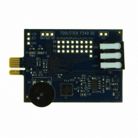
Manufacturer Part Number
TOOLSTICK540DC
Description
DAUGHTER CARD TOOLSTICK F540
Manufacturer
Silicon Laboratories Inc
Series
ToolStickr
Type
MCUr
Datasheets
1.TOOLSTICK540DC.pdf
(274 pages)
2.TOOLSTICK540DC.pdf
(16 pages)
3.TOOLSTICK540DC.pdf
(12 pages)
Specifications of TOOLSTICK540DC
Contents
Daughter Card
Processor To Be Evaluated
C8051F54x
Processor Series
C8051F54x
Interface Type
USB
Operating Supply Voltage
2.7 V to 3.6 V
Lead Free Status / RoHS Status
Lead free / RoHS Compliant
For Use With/related Products
C8051F54x
For Use With
336-1345 - TOOLSTICK BASE ADAPTER336-1182 - ADAPTER USB DEBUG FOR C8051FXXX
Lead Free Status / Rohs Status
Lead free / RoHS Compliant
Other names
336-1717


SFR Definition 22.3. SPI0CKR: SPI0 Clock Rate
SFR Address = 0xA2; SFR Page = 0x00
SFR Definition 22.4. SPI0DAT: SPI0 Data
SFR Address = 0xA3; SFR Page = 0x00
Name
Reset
Name
Reset
Bit
7:0
Bit
7:0
Type
Type
Bit
Bit
SPI0DAT[7:0] SPI0 Transmit and Receive Data.
SCR[7:0]
Name
Name
7
0
7
0
SPI0 Clock Rate.
These bits determine the frequency of the SCK output when the SPI0 module is
configured for master mode operation. The SCK clock frequency is a divided ver-
sion of the system clock, and is given in the following equation, where SYSCLK is
the system clock frequency and SPI0CKR is the 8-bit value held in the SPI0CKR
register.
for 0 <= SPI0CKR <= 255
Example: If SYSCLK = 2 MHz and SPI0CKR = 0x04,
The SPI0DAT register is used to transmit and receive SPI0 data. Writing data to
SPI0DAT places the data into the transmit buffer and initiates a transfer when in
Master Mode. A read of SPI0DAT returns the contents of the receive buffer.
f SCK
f SCK
6
0
6
0
=
=
----------------------------- -
2
--------------------------------------------------------------- -
2
2000000
x
x
5
0
5
0
4
SPI0CKR[7:0]
+
SYSCLK
1
Rev. 1.1
SPI0DAT[7:0]
4
0
4
0
SCR[7:0]
f SCK
+
R/W
R/W
1
Function
Function
=
3
0
3
0
200 kHz
2
0
2
0
C8051F54x
1
0
1
0
0
0
0
0
223
Related parts for TOOLSTICK540DC
Image
Part Number
Description
Manufacturer
Datasheet
Request
R

Part Number:
Description:
KIT TOOL EVAL SYS IN A USB STICK
Manufacturer:
Silicon Laboratories Inc
Datasheet:

Part Number:
Description:
TOOLSTICK DEBUG ADAPTER
Manufacturer:
Silicon Laboratories Inc
Datasheet:

Part Number:
Description:
TOOLSTICK BASE ADAPTER
Manufacturer:
Silicon Laboratories Inc
Datasheet:

Part Number:
Description:
TOOLSTICK DAUGHTER CARD
Manufacturer:
Silicon Laboratories Inc
Datasheet:

Part Number:
Description:
TOOLSTICK DAUGHTER CARD
Manufacturer:
Silicon Laboratories Inc
Datasheet:

Part Number:
Description:
TOOLSTICK DAUGHTER CARD
Manufacturer:
Silicon Laboratories Inc
Datasheet:

Part Number:
Description:
TOOLSTICK PROGRAMMING ADAPTER
Manufacturer:
Silicon Laboratories Inc
Datasheet:

Part Number:
Description:
TOOLSTICK DAUGHTER CARD
Manufacturer:
Silicon Laboratories Inc
Datasheet:

Part Number:
Description:
KIT STARTER TOOLSTICK
Manufacturer:
Silicon Laboratories Inc
Datasheet:

Part Number:
Description:
KIT UNIVERSITY TOOLSTICK STARTER
Manufacturer:
Silicon Laboratories Inc
Datasheet:

Part Number:
Description:
DAUGHTER CARD TOOLSTICK F330
Manufacturer:
Silicon Laboratories Inc
Datasheet:

Part Number:
Description:
CARD DAUGHTER UNIVRSTY TOOLSTICK
Manufacturer:
Silicon Laboratories Inc
Datasheet:

Part Number:
Description:
DAUGHTER CARD TOOLSTICK F582
Manufacturer:
Silicon Laboratories Inc
Datasheet:

Part Number:
Description:
DAUGHTER CARD TOOLSTICK F500
Manufacturer:
Silicon Laboratories Inc
Datasheet:

Part Number:
Description:
DAUGHTER CARD TOOLSTICK F560
Manufacturer:
Silicon Laboratories Inc
Datasheet: