TOOLSTICK540DC Silicon Laboratories Inc, TOOLSTICK540DC Datasheet - Page 198
TOOLSTICK540DC
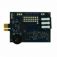
Manufacturer Part Number
TOOLSTICK540DC
Description
DAUGHTER CARD TOOLSTICK F540
Manufacturer
Silicon Laboratories Inc
Series
ToolStickr
Type
MCUr
Datasheets
1.TOOLSTICK540DC.pdf
(274 pages)
2.TOOLSTICK540DC.pdf
(16 pages)
3.TOOLSTICK540DC.pdf
(12 pages)
Specifications of TOOLSTICK540DC
Contents
Daughter Card
Processor To Be Evaluated
C8051F54x
Processor Series
C8051F54x
Interface Type
USB
Operating Supply Voltage
2.7 V to 3.6 V
Lead Free Status / RoHS Status
Lead free / RoHS Compliant
For Use With/related Products
C8051F54x
For Use With
336-1345 - TOOLSTICK BASE ADAPTER336-1182 - ADAPTER USB DEBUG FOR C8051FXXX
Lead Free Status / Rohs Status
Lead free / RoHS Compliant
Other names
336-1717


C8051F54x
20.5.1. Write Sequence (Master)
During a write sequence, an SMBus master writes data to a slave device. The master in this transfer will be
a transmitter during the address byte, and a transmitter during all data bytes. The SMBus interface gener-
ates the START condition and transmits the first byte containing the address of the target slave and the
data direction bit. In this case the data direction bit (R/W) will be logic 0 (WRITE). The master then trans-
mits one or more bytes of serial data. After each byte is transmitted, an acknowledge bit is generated by
the slave. The transfer is ended when the STO bit is set and a STOP is generated. Note that the interface
will switch to Master Receiver Mode if SMB0DAT is not written following a Master Transmitter interrupt.
Figure 20.5 shows a typical master write sequence. Two transmit data bytes are shown, though any num-
ber of bytes may be transmitted. Notice that all of the ‘data byte transferred’ interrupts occur after the ACK
cycle in this mode.
198
S
Received by SMBus
Interface
Transmitted by
SMBus Interface
SLA
Figure 20.5. Typical Master Write Sequence
W
A
Data Byte
Rev. 1.1
Interrupts
A
S = START
P = STOP
A = ACK
W = WRITE
SLA = Slave Address
Data Byte
A
P
Related parts for TOOLSTICK540DC
Image
Part Number
Description
Manufacturer
Datasheet
Request
R

Part Number:
Description:
KIT TOOL EVAL SYS IN A USB STICK
Manufacturer:
Silicon Laboratories Inc
Datasheet:

Part Number:
Description:
TOOLSTICK DEBUG ADAPTER
Manufacturer:
Silicon Laboratories Inc
Datasheet:

Part Number:
Description:
TOOLSTICK BASE ADAPTER
Manufacturer:
Silicon Laboratories Inc
Datasheet:

Part Number:
Description:
TOOLSTICK DAUGHTER CARD
Manufacturer:
Silicon Laboratories Inc
Datasheet:

Part Number:
Description:
TOOLSTICK DAUGHTER CARD
Manufacturer:
Silicon Laboratories Inc
Datasheet:

Part Number:
Description:
TOOLSTICK DAUGHTER CARD
Manufacturer:
Silicon Laboratories Inc
Datasheet:

Part Number:
Description:
TOOLSTICK PROGRAMMING ADAPTER
Manufacturer:
Silicon Laboratories Inc
Datasheet:

Part Number:
Description:
TOOLSTICK DAUGHTER CARD
Manufacturer:
Silicon Laboratories Inc
Datasheet:

Part Number:
Description:
KIT STARTER TOOLSTICK
Manufacturer:
Silicon Laboratories Inc
Datasheet:

Part Number:
Description:
KIT UNIVERSITY TOOLSTICK STARTER
Manufacturer:
Silicon Laboratories Inc
Datasheet:

Part Number:
Description:
DAUGHTER CARD TOOLSTICK F330
Manufacturer:
Silicon Laboratories Inc
Datasheet:

Part Number:
Description:
CARD DAUGHTER UNIVRSTY TOOLSTICK
Manufacturer:
Silicon Laboratories Inc
Datasheet:

Part Number:
Description:
DAUGHTER CARD TOOLSTICK F582
Manufacturer:
Silicon Laboratories Inc
Datasheet:

Part Number:
Description:
DAUGHTER CARD TOOLSTICK F500
Manufacturer:
Silicon Laboratories Inc
Datasheet:

Part Number:
Description:
DAUGHTER CARD TOOLSTICK F560
Manufacturer:
Silicon Laboratories Inc
Datasheet: