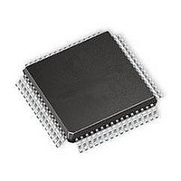
PIC18F65K90T-I/PT Microchip Technology, PIC18F65K90T-I/PT Datasheet - Page 285

PIC18F65K90T-I/PT
Manufacturer Part Number
PIC18F65K90T-I/PT
Description
32kB Flash, 2kB RAM, 1kB EE, NanoWatt XLP, LCD 64 TQFP 10x10x1mm T/R
Manufacturer
Microchip Technology
Series
PIC® XLP™ 18Fr
Datasheet
1.PIC18F66K90-IMR.pdf
(570 pages)
Specifications of PIC18F65K90T-I/PT
Processor Series
PIC18F
Core
PIC
Data Bus Width
8 bit
Program Memory Type
Flash
Program Memory Size
32 KB
Data Ram Size
2 KB
Interface Type
I2C, SPI
Maximum Clock Frequency
64 MHz
Number Of Timers
8
Operating Supply Voltage
1.8 V to 5.5 V
Maximum Operating Temperature
+ 125 C
3rd Party Development Tools
52715-96, 52716-328, 52717-734, 52712-325, EWPIC18
Minimum Operating Temperature
- 40 C
On-chip Adc
12 bit, 16 Channel
Core Processor
PIC
Core Size
8-Bit
Speed
64MHz
Connectivity
I²C, LIN, SPI, UART/USART
Peripherals
Brown-out Detect/Reset, LCD, POR, PWM, WDT
Number Of I /o
53
Eeprom Size
1K x 8
Ram Size
2K x 8
Voltage - Supply (vcc/vdd)
1.8 V ~ 5.5 V
Data Converters
A/D 16x12b
Oscillator Type
Internal
Operating Temperature
-40°C ~ 85°C
Package / Case
64-TQFP
Lead Free Status / Rohs Status
Details
Available stocks
Company
Part Number
Manufacturer
Quantity
Price
Company:
Part Number:
PIC18F65K90T-I/PT
Manufacturer:
Microchip Technology
Quantity:
10 000
Company:
Part Number:
PIC18F65K90T-I/PTRSL
Manufacturer:
Microchip Technology
Quantity:
10 000
- Current page: 285 of 570
- Download datasheet (5Mb)
20.3.2.3
Under firmware control, an internal reference for the
LCD bias voltages can be enabled. When enabled, the
source of this voltage can be V
When no internal reference is selected, the LCD
contrast control circuit is disabled and LCD bias must
be provided externally. Whenever the LCD module is
inactive (LCDA = 0), the internal reference will be
turned off.
20.3.2.4
The VLCD3, VLCD2 and VLCD1 pins provide the
ability for an external LCD bias network to be used
instead of the internal ladder. Use of the VLCDx pins
does not prevent use of the internal ladder.
Each VLCD pin has an independent control in the
LCDREF register, allowing access to any or all of the
LCD bias signals.
This architecture allows for maximum flexibility in
different applications. The VLCDx pins could be used
to add capacitors to the internal reference ladder for
increasing the drive capacity. For applications where
the internal contrast control is insufficient, the firmware
can choose to enable only the VLCD3 pin, allowing an
external contrast control circuit to use the internal
reference divider.
20.4
The LCD driver module can be configured into four
multiplex types:
• Static (only COM0 used)
• 1/2 multiplex (COM0 and COM1 are used)
• 1/3 multiplex (COM0, COM1 and COM2 are used)
• 1/4 multiplex (COM0, COM1, COM2 and COM3 are
The LMUX<1:0> setting (LCDCON<1:0>) decides the
function of the PORTE<6:4> bits. (For details, see
Table
2009-2011 Microchip Technology Inc.
used)
20-4.)
LCD Multiplex Types
Internal Reference
VLCDx Pins
DD
.
PIC18F87K90 FAMILY
If the pin is a digital I/O, the corresponding TRIS bit
controls the data direction. If the pin is a COM drive, the
TRIS setting of that pin is overridden.
TABLE 20-4:
20.5
The LCDSEx registers are used to select the pin
function for each segment pin. The selection allows
each pin to operate as either an LCD segment driver or
a digital only pin. To configure the pin as a segment pin,
the corresponding bits in the LCDSEx registers must
be set to ‘1’.
If the pin is a digital I/O, the corresponding TRIS bit
controls the data direction. Any bit set in the LCDSEx
registers overrides any bit settings in the corresponding
TRIS register.
20.6
The LCDDATAx registers contain bits that define the
state of each pixel. Each bit defines one unique pixel.
Table 20-2
LCDDATAx registers to the respective common and
segment signals.
Any LCD pixel location not being used for display can
be used as general purpose RAM.
LMUX<1:0> PORTE<6>
Note:
Note:
00
01
10
11
Segment Enables
Pixel Control
shows the correlation of each bit in the
On a Power-on Reset, the LMUX<1:0>
bits are ‘00’.
On a Power-on Reset, these pins are
configured as digital I/O.
COM3 Driver COM2 Driver COM1 Driver
Digital I/O
Digital I/O
Digital I/O
PORTE<6:4> FUNCTION
COM2 Driver COM1 Driver
PORTE<5>
Digital I/O
Digital I/O
DS39957D-page 285
COM1 Driver
PORTE<4>
Digital I/O
Related parts for PIC18F65K90T-I/PT
Image
Part Number
Description
Manufacturer
Datasheet
Request
R

Part Number:
Description:
Manufacturer:
Microchip Technology Inc.
Datasheet:

Part Number:
Description:
Manufacturer:
Microchip Technology Inc.
Datasheet:

Part Number:
Description:
Manufacturer:
Microchip Technology Inc.
Datasheet:

Part Number:
Description:
Manufacturer:
Microchip Technology Inc.
Datasheet:

Part Number:
Description:
Manufacturer:
Microchip Technology Inc.
Datasheet:

Part Number:
Description:
Manufacturer:
Microchip Technology Inc.
Datasheet:

Part Number:
Description:
Manufacturer:
Microchip Technology Inc.
Datasheet:

Part Number:
Description:
Manufacturer:
Microchip Technology Inc.
Datasheet:


