PIC18F65K90T-I/PT Microchip Technology, PIC18F65K90T-I/PT Datasheet - Page 112
PIC18F65K90T-I/PT
Manufacturer Part Number
PIC18F65K90T-I/PT
Description
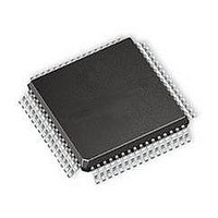
32kB Flash, 2kB RAM, 1kB EE, NanoWatt XLP, LCD 64 TQFP 10x10x1mm T/R
Manufacturer
Microchip Technology
Series
PIC® XLP™ 18Fr
Datasheet
1.PIC18F66K90-IMR.pdf
(570 pages)
Specifications of PIC18F65K90T-I/PT
Processor Series
PIC18F
Core
PIC
Data Bus Width
8 bit
Program Memory Type
Flash
Program Memory Size
32 KB
Data Ram Size
2 KB
Interface Type
I2C, SPI
Maximum Clock Frequency
64 MHz
Number Of Timers
8
Operating Supply Voltage
1.8 V to 5.5 V
Maximum Operating Temperature
+ 125 C
3rd Party Development Tools
52715-96, 52716-328, 52717-734, 52712-325, EWPIC18
Minimum Operating Temperature
- 40 C
On-chip Adc
12 bit, 16 Channel
Core Processor
PIC
Core Size
8-Bit
Speed
64MHz
Connectivity
I²C, LIN, SPI, UART/USART
Peripherals
Brown-out Detect/Reset, LCD, POR, PWM, WDT
Number Of I /o
53
Eeprom Size
1K x 8
Ram Size
2K x 8
Voltage - Supply (vcc/vdd)
1.8 V ~ 5.5 V
Data Converters
A/D 16x12b
Oscillator Type
Internal
Operating Temperature
-40°C ~ 85°C
Package / Case
64-TQFP
Lead Free Status / Rohs Status
Details
Available stocks
Company
Part Number
Manufacturer
Quantity
Price
Company:

Part Number:
PIC18F65K90T-I/PT
Manufacturer:
Microchip Technology
Quantity:
10 000
Company:
Part Number:
PIC18F65K90T-I/PTRSL
Manufacturer:
Microchip Technology
Quantity:
10 000


PIC18F87K90 FAMILY
FIGURE 7-2:
7.2
Several control registers are used in conjunction with
the TBLRD and TBLWT instructions. These include the:
• EECON1 register
• EECON2 register
• TABLAT register
• TBLPTR registers
7.2.1
The EECON1 register
register for memory accesses. The EECON2 register,
not a physical register, is used exclusively in the
memory
EECON2 will read all ‘0’s.
The EEPGD control bit determines if the access is a
program or data EEPROM memory access. When
clear, any subsequent operations operate on the data
EEPROM memory. When set, any subsequent
operations operate on the program memory.
The CFGS control bit determines if the access is to the
Configuration/Calibration registers or to program
memory/data
subsequent operations operate on Configuration
registers regardless of EEPGD (see
“Special Features of the
selection access is determined by EEPGD.
DS39957D-page 112
Note 1: The Table Pointer actually points to one of 64 holding registers; the address of which is determined by
Control Registers
write
TBLPTRU
EECON1 AND EECON2 REGISTERS
EEPROM
TBLPTRL<5:0>. The process for physically writing data to the program memory array is discussed in
Section 7.5 “Writing to Flash Program
and
Table Pointer
TABLE WRITE OPERATION
TBLPTRH
erase
(Register
CPU”). When clear, memory
memory.
sequences.
(1)
TBLPTRL
7-1) is the control
Program Memory
(TBLPTR)
Section 28.0
When
Reading
set,
Memory”.
Instruction:
Holding Registers
Program Memory
The FREE bit, when set, allows a program memory
erase operation. When FREE is set, the erase
operation is initiated on the next WR command. When
FREE is clear, only writes are enabled.
The WREN bit, when set, allows a write operation. On
power-up, the WREN bit is clear. The WRERR bit is set
in hardware when the WR bit is set and cleared when
the internal programming timer expires and the write
operation is complete.
The WR control bit initiates write operations. The bit
cannot be cleared, only set, in software. It is cleared in
hardware at the completion of the write operation.
TBLWT
Note:
Note:
*
During normal operation, the WRERR is
read as ‘1’. This can indicate that a write
operation was prematurely terminated by
a Reset, or a write operation was
attempted improperly.
The EEIF interrupt flag bit (PIR6<4>) is
set when the write is complete. It must be
cleared in software.
2009-2011 Microchip Technology Inc.
Table Latch (8-bit)
TABLAT
Related parts for PIC18F65K90T-I/PT
Image
Part Number
Description
Manufacturer
Datasheet
Request
R

Part Number:
Description:
Manufacturer:
Microchip Technology Inc.
Datasheet:
Part Number:
Description:
Manufacturer:
Microchip Technology Inc.
Datasheet:
Part Number:
Description:
Manufacturer:
Microchip Technology Inc.
Datasheet:
Part Number:
Description:
Manufacturer:
Microchip Technology Inc.
Datasheet:
Part Number:
Description:
Manufacturer:
Microchip Technology Inc.
Datasheet:
Part Number:
Description:
Manufacturer:
Microchip Technology Inc.
Datasheet:
Part Number:
Description:
Manufacturer:
Microchip Technology Inc.
Datasheet:
Part Number:
Description:
Manufacturer:
Microchip Technology Inc.
Datasheet: