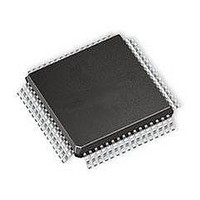
PIC18F65K90T-I/PT Microchip Technology, PIC18F65K90T-I/PT Datasheet - Page 206

PIC18F65K90T-I/PT
Manufacturer Part Number
PIC18F65K90T-I/PT
Description
32kB Flash, 2kB RAM, 1kB EE, NanoWatt XLP, LCD 64 TQFP 10x10x1mm T/R
Manufacturer
Microchip Technology
Series
PIC® XLP™ 18Fr
Datasheet
1.PIC18F66K90-IMR.pdf
(570 pages)
Specifications of PIC18F65K90T-I/PT
Processor Series
PIC18F
Core
PIC
Data Bus Width
8 bit
Program Memory Type
Flash
Program Memory Size
32 KB
Data Ram Size
2 KB
Interface Type
I2C, SPI
Maximum Clock Frequency
64 MHz
Number Of Timers
8
Operating Supply Voltage
1.8 V to 5.5 V
Maximum Operating Temperature
+ 125 C
3rd Party Development Tools
52715-96, 52716-328, 52717-734, 52712-325, EWPIC18
Minimum Operating Temperature
- 40 C
On-chip Adc
12 bit, 16 Channel
Core Processor
PIC
Core Size
8-Bit
Speed
64MHz
Connectivity
I²C, LIN, SPI, UART/USART
Peripherals
Brown-out Detect/Reset, LCD, POR, PWM, WDT
Number Of I /o
53
Eeprom Size
1K x 8
Ram Size
2K x 8
Voltage - Supply (vcc/vdd)
1.8 V ~ 5.5 V
Data Converters
A/D 16x12b
Oscillator Type
Internal
Operating Temperature
-40°C ~ 85°C
Package / Case
64-TQFP
Lead Free Status / Rohs Status
Details
Available stocks
Company
Part Number
Manufacturer
Quantity
Price
Company:
Part Number:
PIC18F65K90T-I/PT
Manufacturer:
Microchip Technology
Quantity:
10 000
Company:
Part Number:
PIC18F65K90T-I/PTRSL
Manufacturer:
Microchip Technology
Quantity:
10 000
- Current page: 206 of 570
- Download datasheet (5Mb)
PIC18F87K90 FAMILY
15.3
Timer3/5/7 can be configured for 16-bit reads and
writes (see
(TxCON<1>) is set, the address for TMRxH is mapped
to a buffer register for the high byte of Timer3/5/7. A
read from TMRxL will load the contents of the high byte
of Timer3/5/7 into the Timerx High Byte Buffer register.
This provides users with the ability to accurately read
all 16 bits of Timer3/5/7 without having to determine
whether a read of the high byte, followed by a read of
the low byte, has become invalid due to a rollover
between reads.
A write to the high byte of Timer3/5/7 must also take
place through the TMRxH Buffer register. The Timer3/
5/7 high byte is updated with the contents of TMRxH
when a write occurs to TMRxL. This allows users to
write all 16 bits to both the high and low bytes of
Timer3/5/7 at once.
The high byte of Timer3/5/7 is not directly readable or
writable in this mode. All reads and writes must take
place through the Timerx High Byte Buffer register.
Writes to TMRxH do not clear the Timer3/5/7 prescaler.
The prescaler is only cleared on writes to TMRxL.
15.4
The SOSC internal oscillator may be used as the clock
source for Timer3/5/7. The SOSC oscillator is enabled by
setting one of five bits: any of the four SOSCEN bits in the
TxCON registers (TxCON<3>) or the SOSCGO bit in the
OSCCON2 register (OSCCON2<3>). To use it as the
Timer3/5/7 clock source, the TMRxCS bit must also be
set. As previously noted, this also configures Timer3/5/7
to increment on every rising edge of the oscillator source.
The SOSC oscillator is described in
“Timer1
FIGURE 15-2:
DS39957D-page 206
Timer3/5/7
TMRxGE
TxGPOL
TxGVAL
Timer3/5/7 16-Bit Read/Write Mode
Using the SOSC Oscillator as the
Timer3/5/7 Clock Source
Module”.
TxG_IN
TxCKI
Figure
15.3). When the RD16 control bit
TIMER3/5/7 GATE COUNT ENABLE MODE
N
Section 13.0
N + 1
current count. See
15.5
Timer3/5/7 can be configured to count freely or the
count can be enabled and disabled using the Timer3/
5/7 gate circuitry. This is also referred to as the
Timer3/5/7 gate count enable.
The Timer3/5/7 gate can also be driven by multiple
selectable sources.
15.5.1
The Timerx Gate Enable mode is enabled by setting
the TMRxGE bit (TxGCON<7>). The polarity of the
Timerx Gate Enable mode is configured using the
TxGPOL bit (TxGCON<6>).
When Timerx Gate Enable mode is enabled, Timer3/5/7
will increment on the rising edge of the Timer3/5/7 clock
source. When Timerx Gate Enable mode is disabled, no
incrementing will occur and Timer3/5/7 will hold the
TABLE 15-1:
† The clock on which TMR3/5/7 is running. For more
TxCLK
information, see TxCLK in
(†)
Timer3/5/7 Gates
N + 2
(TxGCON<6>)
TIMER3/5/7 GATE COUNT ENABLE
TxGPOL
0
0
1
1
TIMER3/5/7 GATE ENABLE
SELECTIONS
Figure 15-2
2009-2011 Microchip Technology Inc.
TxG Pin
Figure
N + 3
0
1
0
1
for timing details.
15-1.
Counts
Holds Count
Holds Count
Counts
Timerx Operation
N + 4
Related parts for PIC18F65K90T-I/PT
Image
Part Number
Description
Manufacturer
Datasheet
Request
R

Part Number:
Description:
Manufacturer:
Microchip Technology Inc.
Datasheet:

Part Number:
Description:
Manufacturer:
Microchip Technology Inc.
Datasheet:

Part Number:
Description:
Manufacturer:
Microchip Technology Inc.
Datasheet:

Part Number:
Description:
Manufacturer:
Microchip Technology Inc.
Datasheet:

Part Number:
Description:
Manufacturer:
Microchip Technology Inc.
Datasheet:

Part Number:
Description:
Manufacturer:
Microchip Technology Inc.
Datasheet:

Part Number:
Description:
Manufacturer:
Microchip Technology Inc.
Datasheet:

Part Number:
Description:
Manufacturer:
Microchip Technology Inc.
Datasheet:


