CYIL1SM4000AA-GDC Cypress Semiconductor Corp, CYIL1SM4000AA-GDC Datasheet - Page 17
CYIL1SM4000AA-GDC
Manufacturer Part Number
CYIL1SM4000AA-GDC
Description
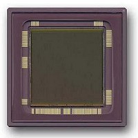
SENSOR IMAGE 4MP CMOS 127-PGA
Manufacturer
Cypress Semiconductor Corp
Type
CMOS Imagingr
Datasheet
1.CYIL1SM4000-EVAL.pdf
(32 pages)
Specifications of CYIL1SM4000AA-GDC
Package / Case
127-PGA
Pixel Size
12µm x 12µm
Active Pixel Array
2048H x 2048V
Frames Per Second
15
Voltage - Supply
2.5V, 3.3V
Operating Supply Voltage
2.5 V
Maximum Operating Temperature
+ 60 C
Minimum Operating Temperature
0 C
Image Size
2048 H x 2048 V
Color Sensing
Monochrome
Package
127CPGA
Operating Temperature
0 to 60 °C
Lead Free Status / RoHS Status
Contains lead / RoHS non-compliant
Lead Free Status / RoHS Status
Lead free / RoHS Compliant, Contains lead / RoHS non-compliant
Other names
LUPA-4000-M
LUPA-4000-M
LUPA-4000-M


In the figure, shown from bottom to top: Clock_x, Sync_x and
output. Output level before the first pixel is the level of the last
pixel on previous line.
As soon as Sync_x is high and one rising edge of Clock_x
occurs, the pixels are brought to the analog outputs. This is again
the simulation result of a comparable sensor to show the
principle.
Note the time difference between the clock edge and the
moment the data is seen at the output. Because it is dificult to
predict this time difference in advance, have the ADC sampling
clock flexible to set an optimal ‘add sampling’ point. The time
differences can easily vary between 5 ns and 15 ns and must be
tested on the real devices.
In this case, the control signals Norowsel and pre_col are made
active for about 20 ns from the moment the next line is selected.
The time these pulses must be active is related to the biasing
resistance Pre_load. The lower this resistance, the shorter the
pulse duration of Norowsel and pre_col may be. After these
pulses are given, wait for at least 180 ns before the first pixel is
sampled. For this mode Sh_col must be made active (low) all the
time.
Document Number: 38-05712 Rev. *F
Figure 19. Standard Timing for ROT (only pre_col and No_row_sel control signals are required)
Figure 18. Output Signal Related to Clock_x Signal
dark
Pixel 1
Pixel2….: Pixel period : 20nsec
Reduced ROT Timing
The ROT is the time between the selection of lines that you must
wait to get the data stable at the column amplifiers. It is a loss in
time, which should be reduced as much as possible.
Standard Timing (200 ns)
In this case, the control signals Norowsel and pre_col are made
active for about 20 ns from the moment the next line is selected.
The time these pulses must be active is related to the biasing
resistance Pre_load. The lower this resistance, the shorter the
pulse duration of Norowsel and pre_col may be. After these
pulses are given, wait for at least 180 ns before the first pixel is
sampled. For this mode, Sh_col must always be active (low).
Backup Timing (ROT = 100 to 200 ns)
Use a sample and hold function to reduce the ROT.
Track the analog data using Sh_col during the first 100 ns during
the selection of a new set of lines. After 100 ns, the analog data
is stored. The ROT is reduced to 100 ns, but as the internal data
is not stable yet, dynamic range is lost. This is because the
complete analog levels are not reached after 100 ns.
saturated
CYIL1SM4000AA
Clock_x:
25MHz
Output 1
Sync_x
Page 17 of 32
Related parts for CYIL1SM4000AA-GDC
Image
Part Number
Description
Manufacturer
Datasheet
Request
R

Part Number:
Description:
Manufacturer:
Cypress Semiconductor Corp
Datasheet:
Part Number:
Description:
Manufacturer:
Cypress Semiconductor Corp
Datasheet:
Part Number:
Description:
Manufacturer:
Cypress Semiconductor Corp
Datasheet:
Part Number:
Description:
Manufacturer:
Cypress Semiconductor Corp
Datasheet:
Part Number:
Description:
Manufacturer:
Cypress Semiconductor Corp
Datasheet: