CYIL1SM4000AA-GDC Cypress Semiconductor Corp, CYIL1SM4000AA-GDC Datasheet - Page 13
CYIL1SM4000AA-GDC
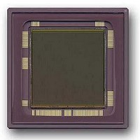
Manufacturer Part Number
CYIL1SM4000AA-GDC
Description
SENSOR IMAGE 4MP CMOS 127-PGA
Manufacturer
Cypress Semiconductor Corp
Type
CMOS Imagingr
Datasheet
1.CYIL1SM4000-EVAL.pdf
(32 pages)
Specifications of CYIL1SM4000AA-GDC
Package / Case
127-PGA
Pixel Size
12µm x 12µm
Active Pixel Array
2048H x 2048V
Frames Per Second
15
Voltage - Supply
2.5V, 3.3V
Operating Supply Voltage
2.5 V
Maximum Operating Temperature
+ 60 C
Minimum Operating Temperature
0 C
Image Size
2048 H x 2048 V
Color Sensing
Monochrome
Package
127CPGA
Operating Temperature
0 to 60 °C
Lead Free Status / RoHS Status
Contains lead / RoHS non-compliant
Lead Free Status / RoHS Status
Lead free / RoHS Compliant, Contains lead / RoHS non-compliant
Other names
LUPA-4000-M
LUPA-4000-M
LUPA-4000-M


Timing and Readout of Image Sensor
The timing of the LUPA 4000 sensor consists of two parts. The
first part is related to the control of the pixels, the integration time,
and the signal level. The second part is related to the readout of
the image sensor. As full synchronous shutter is possible with
this image sensor, integration time and readout can be in parallel
or sequential.
In the parallel mode, the integration time of the frame I is ongoing
during readout of frame I-1.
structure.
The control of the frame’s readout and integration time are
independent of each other with the only exception that the end
of the integration time from frame I+1 is the beginning of the
readout of frame I+1.
Timing of Pixel Array
The first part of the timing is related to the timing of the pixel array. This implies control of integration time, synchronous shutter
operation, and sampling of the pixel information onto the memory element inside each pixel. The signals required for this control are
described in
Figure 14
signals Mem_hl, precharge, and sample must be given. The reset signal controls the integration time, which is defined as the time
between the falling edge of reset and the rising edge of sample.
The integration time is determined by the falling edge of the reset pulse. The longer the pulse is high, the shorter the integration time.
At the end of the integration time, the information must be stored onto the memory element for readout.
Document Number: 38-05712 Rev. *F
shows the external applied signals required to control the pixel array. At the end of the integration time from frame I+1, the
Pixel Array Signals
Integration Frame I
Figure 12
and in
shows this parallel timing
Figure
Figure 13. Integration and Readout in Sequence
11.
Read Frame I
Figure 14. Pixel Array Timing
Figure 12. Integration and Readout in Parallel
The LUPA 4000 sensor is also used in sequential mode
(triggered snapshot mode) where readout and integration is
sequential.
Integration I+1
Figure 13
Read Frame I
Integration I+1
shows this sequential timing.
Read Frame I+1
CYIL1SM4000AA
Read Frame I+1
Integration I+2
Page 13 of 32
Related parts for CYIL1SM4000AA-GDC
Image
Part Number
Description
Manufacturer
Datasheet
Request
R

Part Number:
Description:
Manufacturer:
Cypress Semiconductor Corp
Datasheet:
Part Number:
Description:
Manufacturer:
Cypress Semiconductor Corp
Datasheet:
Part Number:
Description:
Manufacturer:
Cypress Semiconductor Corp
Datasheet:
Part Number:
Description:
Manufacturer:
Cypress Semiconductor Corp
Datasheet:
Part Number:
Description:
Manufacturer:
Cypress Semiconductor Corp
Datasheet: