CYIL1SM4000AA-GDC Cypress Semiconductor Corp, CYIL1SM4000AA-GDC Datasheet
CYIL1SM4000AA-GDC
Specifications of CYIL1SM4000AA-GDC
LUPA-4000-M


Related parts for CYIL1SM4000AA-GDC

CYIL1SM4000AA-GDC Summary of contents
Page 1
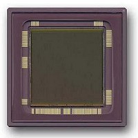
... Applications Intelligent traffic system ■ High speed machine vision ■ Ordering Information Marketing Part Number CYIL1SM4000AA-GDC CYIL1SC4000AA-GDC CYIL1SM4000-EVAL Note Refer to Ordering Code Definition Cypress Semiconductor Corporation Document Number: 38-05712 Rev. *F Overview The LUPA 4000 is a CMOS image sensor (CIS) with a 4.0 megapixel resolution 2048 × ...
Page 2
... Non Destructive Readout (NDR) ....................................9 Operation and Signaling .....................................................9 Power Supplies and Ground ..........................................9 Biasing and Analog Signals ............................................10 Pixel Array Signals .........................................................10 Document Number: 38-05712 Rev. *F CYIL1SM4000AA Digital Signals .................................................................11 Test Signals ....................................................................12 Frame Rate and Windowing ...........................................12 Timing and Readout of Image Sensor ...............................13 Timing of Pixel Array ......................................................13 Readout of Image Sensor ..............................................14 Serial Peripheral Interface ...
Page 3
... ABS rating for 2.5-V supply group ABS rating for 3.3-V supply group Operating temperature range Storage temperature range Storage humidity range Human body model (HBM) Charged device model (CDM) Latch-up rating CYIL1SM4000AA Parameter Specification 15 fps at full resolution - 11.5 µV/e 2 1550 (V/s)/(W ...
Page 4
... This device contains circuitry to protect the inputs against damage due to high static voltages or electric fields. However recommended that normal precautions. be taken to avoid application of any voltages higher than the maximum rated voltages to this high-impedance circuit. Document Number: 38-05712 Rev all other limits T = +30 °C MAX J Description CYIL1SM4000AA [7] Min Typ Max Units –10% 2.5 +10% V – ...
Page 5
... The color version of LUPA 4000 is available in Bayer (RGB) patterned color filter array. The orientation of RGB is shown in Figure 2. Figure 3. Spectral Response Curve for Mono and Color Document Number: 38-05712 Rev. *F CYIL1SM4000AA Figure 2. Color Filter Array LUPA 4000 Pixel Array G B x_readout direction ...
Page 6
... Figure 5. Output Stage Architecture. Image Sensor SPI The output voltage of Output1 is between 1.3 V (dark level) and 0.3 V (white level) and depends on process variations and voltage supply settings. The output voltage of Output2 is determined by the DAC. CYIL1SM4000AA Eos_x Output 1 (Pixel Signal) 7 bits Output 2 DAC ...
Page 7
... The ADC converts the pixel data on the falling edge of the ADC_CLOCK, but it takes two clock cycles before this pixel data is at the output of the ADC. This pipeline delay is shown in Figure 6. Figure 6. ADC Timing 200 ns CYIL1SM4000AA Specification [ bits 10 Msamples/s Typ < 0.4 LSB RMS Typ < ...
Page 8
... Reset Reset Exposure Time N FOT N N+1 Readout Frame N-1 FOT Line Readout CYIL1SM4000AA shows the integration and readout sequence for the Common Sample & Hold Time Integration Time Burst Readout Time Exposure Time N+1 FOT Readout Frame N ...
Page 9
... To avoid latch-up of the sensor, follow this sequence: 1. Apply Vdd 2. Apply clocks and digital pulses to the sensor to count 1024 clock_x and 2048 clock_y pulses to empty the shift registers 3. Apply other supplies CYIL1SM4000AA Electrical Specifications Page ...
Page 10
... This signal is also a standard digital level between 0 V and 2.5 V. Vmem: This signal increases the information on the memory element with a certain offset. This increases the output voltage variation. Vmem changes between Vmem_l (2.5 V) and Vmem_h (3.3 V). CYIL1SM4000AA Related Module DC Level Output stage 0.7 V X-addressing ...
Page 11
... MHz. Spi_data (AH ■ Spi_clock (AH ■ data into the SPI register. Spi_load (AH ■ data is internally available on the rising edge of SPI_load. CYIL1SM4000AA Low DC Level High DC Level Vpre_l Controlled by bias-resistor Gnd Vdd Gnd Vres and Vres_ds Vmem_l Vmem_h [10] ): Starts the readout of the frame ...
Page 12
... The size of both address registers is 10-bits. For instance, when the addresses 0000000001 and 0000000001 are uploaded, the readout starts at line 2 and column 2. Frame Readout Time [mS 210 CYIL1SM4000AA Comment 67 Full resolution. 32 Subsample in X-direction. 16 ROI read out. 4.7 ROI read out ...
Page 13
... Figure 13. Integration and Readout in Sequence Read Frame I Integration I+1 Figure 11. Figure 14. Pixel Array Timing CYIL1SM4000AA Read Frame I Read Frame I+1 Integration I+1 Integration I+2 Figure 13 shows this sequential timing. Read Frame I+1 Page ...
Page 14
... Readout frame I Integration I+2 Readout Lines Readout Pixels Figure 14 CYIL1SM4000AA shows the top level concept of this timing. The readout L2048 C2048 shows that at this time Mem_hl is low (typically Page ...
Page 15
... Clock_x is low, the next pixel is selected. Consequently, during one complete period of Clock_x two pixels are read out by the output amplifier. If two analog outputs are used each Clock-X period one pixel is presented at each output. CYIL1SM4000AA Figure 16. This is the time to get Page ...
Page 16
... In this figure, the pixel clock has a frequency of 50 MHz, which results in a pixel rate of 100 Msamples/sec. Figure 18 on page 17 shows the relation between the applied Clock_x and the output signal. CYIL1SM4000AA Page ...
Page 17
... After 100 ns, the analog data is stored. The ROT is reduced to 100 ns, but as the internal data is not stable yet, dynamic range is lost. This is because the complete analog levels are not reached after 100 ns. CYIL1SM4000AA Output 1 Sync_x Clock_x: ...
Page 18
... MΩ). Figure 21. X and Y Addressing with Precharging of Buses Document Number: 38-05712 Rev. *F CYIL1SM4000AA If voltage-averaging is required, the sensor must work in this mode with Sh_col signal and a voltage-averaging signal must be generated after Sh_col drops and before the readout starts (see ...
Page 19
... Output Bit 25 is LSB Figure 22. SPI Block Diagram and Timing 32 outputs to sensor Bit 31 spi_in Clock_spi Entire uploadable block Load_addr Clock_spi spi_in B0 B1 Load_addr CYIL1SM4000AA Value >20 ns >0 ns >0 ns >50 ns >50 ns >20 ns > short as possible Remarks Bit 0 B2 B31 command applied to ...
Page 20
... Vaa and decouple with C = 100 nF to gnda. Input Analog reference input. Biasing for Y-addressing. Connect with MΩ to Vdd and decouple with C = 100 nF to gndd. Supply Power supply digital modules. Ground Ground digital modules. Input Digital input. Control signal to reduce readout time. CYIL1SM4000AA Description Page ...
Page 21
... kΩand decouple with C = 100 nF to gnda. Input Analog reference input. High reference voltage of ADC. See Figure 7 on page 8 for exact resistor value. Supply Power supply reset drivers. Supply Power supply reset drivers. CYIL1SM4000AA Description Figure 7 for exact DDA DDA Page with with ...
Page 22
... Digital input. Control of Vmem signal in pixel. Input Digital input. Control of Vprecharge signal in pixel. Input Digital input. Control of Vsample signal in pixel. Testpin Cathode of temperature diode. Testpin Anode of temperature diode. CYIL1SM4000AA Description with kΩ and decouple DDA DDA Figure 7 on page Page with ...
Page 23
... Digital input. Control signal to reduce readout time. Input Analog reference input. Biasing for Y-addressing. Supply Power supply pixel array. Supply Power supply column modules. Ground Ground analog modules. Supply Power supply analog modules. Ground Ground digital modules. or GND). DD CYIL1SM4000AA Description Table 3 on page 10 for Page ...
Page 24
... Package Drawing Figure 23. LUPA 4000: 127 Pin PGA Package Drawing Document Number: 38-05712 Rev. *F CYIL1SM4000AA 001-07580 *C Page ...
Page 25
... Cavity pad: 27000 µm X 29007 µm ■ Pixel 0,0 is located at 478 µm from the left hand side of the die and 1366 µm from the bottom side of the die. ■ Figure 24. Bonding Pads Diagram of the LUPA 4000 Package Document Number: 38-05712 Rev. *F CYIL1SM4000AA Figure 24. 001-48359 ** Page ...
Page 26
... Products returned to Cypress for failure analysis should be handled under these same conditions and packed in its original packing materials, or the customer may be liable for the product 4000 CYIL1SM4000AA C = Commercial Temperature Range D: D263 Glass Package PGA Revision: A Function: A Resolution: 4 Megapixels Page ...
Page 27
... HBM Human Body Model HMUX horizontal multiplexer I2C inter-integrated circuit IEEE Institute of Electrical and Electronics Engineers IMG regular pixel data Document Number: 38-05712 Rev. *F CYIL1SM4000AA Acronym Description INL integral nonlinearity IP intellectual property JTAG Joint Test Action Group LE line end LS ...
Page 28
... FPN under illumination. QE Quantum efficiency. This parameter characterizes the effectiveness of a pixel in capturing photons and converting them into electrons photon wavelength and pixel color dependent. radiometric units Units for light measurement based on physics. Document Number: 38-05712 Rev. *F CYIL1SM4000AA 1/683 W/m ) ...
Page 29
... Nyquist frequency. temporal noise Noise that varies from frame to frame video stream, temporal noise is visible as twinkling pixels. tint Integration time. Document Number: 38-05712 Rev. *F CYIL1SM4000AA 2 )/sec and are dependent on the 2 ; the units of sensitivity are quoted in V/lux/sec. Note that Page ...
Page 30
... All setting can be adjusted on the fly to evaluate the sensors specifications. Default register values can be loaded to start the software in a desired state. Document Number: 38-05712 Rev. *F Figure 26. Contents of LUPA 4000 Evaluation Kit CYIL1SM4000AA Page ...
Page 31
... Reset pulse Double slope reset pulse Total integration time Document Number: 38-05712 Rev. *F Figure 27. Dual Slope Diagram Read out Reset level 1 p1 Reset level Saturation level Double slope reset time (usually 5- 10% of the total integration time) CYIL1SM4000AA Page ...
Page 32
... Document History Page Document Title: CYIL1SM4000AA LUPA 4000: 4 Megapixel CMOS Image Sensor Document Number: 38-05712 Orig. of Submission Rev. ECN No. Change ** 310396 FPW *A 497132 QGS *B 649219 FPW *C 2738057 NVEA/PYRS *D 2765859 NVEA *E 3006382 NVEA *F 3052567 NVEA Sales, Solutions, and Legal Information Worldwide Sales and Design Support Cypress offers standard and customized CMOS image sensors for consumer as well as industrial and professional applications ...