CYIL1SM4000AA-GDC Cypress Semiconductor Corp, CYIL1SM4000AA-GDC Datasheet - Page 11
CYIL1SM4000AA-GDC
Manufacturer Part Number
CYIL1SM4000AA-GDC
Description
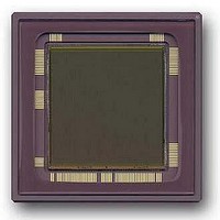
SENSOR IMAGE 4MP CMOS 127-PGA
Manufacturer
Cypress Semiconductor Corp
Type
CMOS Imagingr
Datasheet
1.CYIL1SM4000-EVAL.pdf
(32 pages)
Specifications of CYIL1SM4000AA-GDC
Package / Case
127-PGA
Pixel Size
12µm x 12µm
Active Pixel Array
2048H x 2048V
Frames Per Second
15
Voltage - Supply
2.5V, 3.3V
Operating Supply Voltage
2.5 V
Maximum Operating Temperature
+ 60 C
Minimum Operating Temperature
0 C
Image Size
2048 H x 2048 V
Color Sensing
Monochrome
Package
127CPGA
Operating Temperature
0 to 60 °C
Lead Free Status / RoHS Status
Contains lead / RoHS non-compliant
Lead Free Status / RoHS Status
Lead free / RoHS Compliant, Contains lead / RoHS non-compliant
Other names
LUPA-4000-M
LUPA-4000-M
LUPA-4000-M


In
supplies; for correct polarities of the signals see
signals in
These on-chip drivers need two types of signals to generate the
exact type of signal. It needs digital control signals between 0 V
and 3.3 V (internally converted to 2.5 V) with normal driving
capability and power supplies. The control signals are required
to indicate when they must occur and the power supplies indicate
the level.
Table 4. Overview of Internal and External Pixel Array Signals
For dual slope operation, give a second reset pulse to a lower
reset level during integration. This is done by the control signal
Reset_ds and by the power supply Vres_ds that defines the level
to which the pixel must be reset.
Note that Reset is dominant over Reset_ds, which means that
the high voltage level is applied for reset, if both pulses occur at
the same time.
Multiple slopes are possible having multiple Reset_ds pulses
with a lower Vres_ds level for each pulse given within the same
integration time.
The rise and fall times of the internal generated signals are not
very fast (200 ns). In fact they are made rather slow to limit the
maximum current through the power supply lines (Vmem_h,
Vmem_l, Vres, Vres_ds, Vdd). Current limitation of those power
supplies is not required. However, limit the currents to not higher
than 400 mA.
The power supply Vmem_l must be able to sink this current
because it must be able to discharge the internal capacitance
from the level Vmem_h to the level Vmem_l. The external control
signals should be capable of driving input capacitance of about
10 pF.
Document Number: 38-05712 Rev. *F
Precharge
Sample
Reset
Vmem
Internal Signal
Figure
11, levels are defined by the pixel array voltage
Figure 11
2.0 V to 2.5 V
are generated from the on-chip drivers.
Vlow
0
0
0
2.5 V to 3.3 V
2.5 V to 3.3 V
0.45 V
Vhigh
2.5 V
Figure 11. Internal Timing of Pixel
Table
Reset (AH) and Reset_ds (AH)
External Control Signal
4. The
Precharge (AL)
Mem_hl (AL)
Sample (AL)
Vmem is made of a control signal Mem_hl and 2 supplies
Vmem_h and Vmem_l. If the signal Mem_hl is the logic ‘0’ than
the internal signal Vmem is low, if Mem_hl is logic ‘1’ the internal
signal Vmem is high.
Reset is made with two control signals, Reset and Reset_ds, and
two supplies, Vres and Vres_ds. Depending on the signal that
becomes active, the corresponding supply level is applied to the
pixel.
Table 4
external pixel array signals.
Digital Signals
The digital signals control the readout of the image sensor.
These signals are:
■
■
■
■
■
■
■
Sync_y (AH
synchronises the y-address register: active high. This signal is
also the end of the frame or window and determines the window
width.
Clock_y (AH
this clock, the next line is selected.
Sync_x (AH
address defined by the x-address register. This pulse
synchronises the x-address register: active high. This signal is
also the end of the line and determines the window length.
Clock_x (AH
is required to achieve a pixel rate of 66 MHz.
Spi_data (AH
Spi_clock (AH
data into the SPI register.
Spi_load (AH
data is internally available on the rising edge of SPI_load.
summarizes the relation between the internal and
[10]
[10]
[10]
[10]
[10]
[10]
[10]
): Starts the readout of the selected line at the
): Starts the readout of the frame. This pulse
): Determines the pixel rate. A clock of 33 MHz
): Clock of the y-register. On the rising edge of
): When the SPI register is uploaded, then the
): Data for the SPI.
): Clock of the SPI. This clock downloads the
Low DC Level
Vmem_l
Vpre_l
Gnd
Gnd
CYIL1SM4000AA
Controlled by bias-resistor
Vdd
Vres and Vres_ds
Vmem_h
High DC Level
Page 11 of 32
Related parts for CYIL1SM4000AA-GDC
Image
Part Number
Description
Manufacturer
Datasheet
Request
R

Part Number:
Description:
Manufacturer:
Cypress Semiconductor Corp
Datasheet:
Part Number:
Description:
Manufacturer:
Cypress Semiconductor Corp
Datasheet:
Part Number:
Description:
Manufacturer:
Cypress Semiconductor Corp
Datasheet:
Part Number:
Description:
Manufacturer:
Cypress Semiconductor Corp
Datasheet:
Part Number:
Description:
Manufacturer:
Cypress Semiconductor Corp
Datasheet: