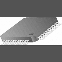
CLC021AVGZ-3.3 National Semiconductor, CLC021AVGZ-3.3 Datasheet - Page 6

CLC021AVGZ-3.3
Manufacturer Part Number
CLC021AVGZ-3.3
Description
IC, DIG VIDEO SERIALIZER, 3.63V, PQFP-44
Manufacturer
National Semiconductor
Datasheet
1.CLC021AVGZ-3.3.pdf
(18 pages)
Specifications of CLC021AVGZ-3.3
Ic Interface Type
Parallel, Serial
Supply Voltage Range
2.97V To 3.63V
Power Dissipation Pd
235mW
Operating Temperature Range
0°C To +70°C
Digital Ic Case Style
PQFP
No. Of Pins
44
Operating Temperature (min)
0C
Operating Temperature Classification
Commercial
Operating Temperature (max)
70C
Package Type
PQFP
Rad Hardened
No
Lead Free Status / RoHS Status
Contains lead / RoHS non-compliant
Lead Free Status / RoHS Status
Contains lead / RoHS non-compliant
Available stocks
Company
Part Number
Manufacturer
Quantity
Price
Company:
Part Number:
CLC021AVGZ-3.3
Manufacturer:
Texas Instruments
Quantity:
10 000
Part Number:
CLC021AVGZ-3.3
Manufacturer:
TI/德州仪器
Quantity:
20 000
Company:
Part Number:
CLC021AVGZ-3.3/NOPB
Manufacturer:
NSC
Quantity:
96
Company:
Part Number:
CLC021AVGZ-3.3/NOPB
Manufacturer:
Texas Instruments
Quantity:
10 000
www.national.com
L
R
Symbol
GEN
AC Electrical Characteristics—CLC021AVGZ-3.3
GEN
Over Supply Voltage and Operating Temperature ranges, unless otherwise specified (Note 3).
Note 1: “Absolute Maximum Ratings” are those parameter values beyond which the life and operation of the device cannot be guaranteed. The stating herein of
these maximums shall not be construed to imply that the device can or should be operated at or beyond these values. The table of “Electrical Characteristics”
specifies acceptable device operating conditions.
Note 2: Current flow into device pins is defined as positive. Current flow out of device pins is defined as negative. All voltages are stated referenced to V
Note 3: Typical values are stated for V
Note 4: Specification is guaranteed by design.
Note 5: R
Note 6: CLC021 mounted in the SD021EVK board, configured in BIST mode (NTSC colour bars) with P
reference. Timing jitter measured with Tektronix VM700T using jitter measurement FFT mode, frame rate, 1 kHz filter bandwidth, Hanning window.
Note 7: Measured from rising-edge of first P
Test Loads
L
= 75Ω, AC-coupled
Output Inductance
Output Resistance
Parameter
@
270 M
DD
bps
= +5.0V (CLC021AVGZ-5.0) or +3.3V (CLC021AVGZ-3.3) and T
, R
CLK
(Note 4)
(Note 4)
REF
cycle until Lock Detect output goes high (true).
= 1.69 kΩ 1%, See Test Loads and Figure 2.
Conditions
FIGURE 1. Test Loads
6
SDO, SDO
Reference
CLK
(Continued)
A
= 27 MHz derived from Tektronix TG2000 black-burst
= +25˚C.
Min
Typ
25k
6
10136803
Max
SS
Units
= 0V.
nH
Ω


