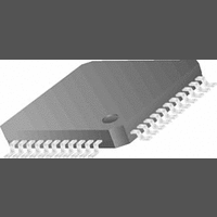
CLC021AVGZ-3.3 National Semiconductor, CLC021AVGZ-3.3 Datasheet - Page 10

CLC021AVGZ-3.3
Manufacturer Part Number
CLC021AVGZ-3.3
Description
IC, DIG VIDEO SERIALIZER, 3.63V, PQFP-44
Manufacturer
National Semiconductor
Datasheet
1.CLC021AVGZ-3.3.pdf
(18 pages)
Specifications of CLC021AVGZ-3.3
Ic Interface Type
Parallel, Serial
Supply Voltage Range
2.97V To 3.63V
Power Dissipation Pd
235mW
Operating Temperature Range
0°C To +70°C
Digital Ic Case Style
PQFP
No. Of Pins
44
Operating Temperature (min)
0C
Operating Temperature Classification
Commercial
Operating Temperature (max)
70C
Package Type
PQFP
Rad Hardened
No
Lead Free Status / RoHS Status
Contains lead / RoHS non-compliant
Lead Free Status / RoHS Status
Contains lead / RoHS non-compliant
Available stocks
Company
Part Number
Manufacturer
Quantity
Price
Company:
Part Number:
CLC021AVGZ-3.3
Manufacturer:
Texas Instruments
Quantity:
10 000
Part Number:
CLC021AVGZ-3.3
Manufacturer:
TI/德州仪器
Quantity:
20 000
Company:
Part Number:
CLC021AVGZ-3.3/NOPB
Manufacturer:
NSC
Quantity:
96
Company:
Part Number:
CLC021AVGZ-3.3/NOPB
Manufacturer:
Texas Instruments
Quantity:
10 000
www.national.com
Device Operation
BUILT-IN SELF-TEST (BIST)
The CLC021 has a built-in self-test (BIST) function. The
BIST performs a comprehensive go/no-go test of the device.
The test uses either a full-field colour bar for NTSC or a PLL
pathological for PAL as the test data pattern. Data is input
internally in the input data register, processed through the
device and tested for errors. A go/no-go indication is given at
the Test_Output. Table 1 gives device pin functions and
Table 2 gives the test pattern codes used for this function.
The signal level at Test_Output, pin 3, indicates a pass or fail
condition.
The BIST is initiated by applying the code for the desired
BIST to D0 through D3 (D9 through D4 are 00h) and a 27
MHz clock at the P
CLK
input. Since all parallel data inputs are
(Continued)
FIGURE 5. Power-On Reset Sequence with Manual Reset
FIGURE 4. Power-On Reset Sequence
10
equipped with an internal pull-down device, only those inputs
D0 through D3 which require a logic-1 need be pulled high.
After the Lock_Detect output goes high indicating the VCO is
locked on frequency, TPG_Enable, pin 29, is taken to a logic
high. The Lock_Detect output may be temporarily connected
to TPG_Enable to automate BIST operation. Test_Output,
pin 3, is monitored for a pass/fail indication. If no errors have
been detected, this output will go to a logic high level ap-
proximately 2 field intervals after TPG_Enable is taken high.
If errors have been detected in the internal circuitry of the
CLC021, Test_Output will remain low until the test is termi-
nated. The BIST is terminated by taking TPG _Enable to a
logic low. Continuous serial data output is available during
the test.
10136815
10136814


