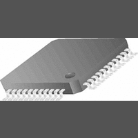
CLC021AVGZ-3.3 National Semiconductor, CLC021AVGZ-3.3 Datasheet - Page 11

CLC021AVGZ-3.3
Manufacturer Part Number
CLC021AVGZ-3.3
Description
IC, DIG VIDEO SERIALIZER, 3.63V, PQFP-44
Manufacturer
National Semiconductor
Datasheet
1.CLC021AVGZ-3.3.pdf
(18 pages)
Specifications of CLC021AVGZ-3.3
Ic Interface Type
Parallel, Serial
Supply Voltage Range
2.97V To 3.63V
Power Dissipation Pd
235mW
Operating Temperature Range
0°C To +70°C
Digital Ic Case Style
PQFP
No. Of Pins
44
Operating Temperature (min)
0C
Operating Temperature Classification
Commercial
Operating Temperature (max)
70C
Package Type
PQFP
Rad Hardened
No
Lead Free Status / RoHS Status
Contains lead / RoHS non-compliant
Lead Free Status / RoHS Status
Contains lead / RoHS non-compliant
Available stocks
Company
Part Number
Manufacturer
Quantity
Price
Company:
Part Number:
CLC021AVGZ-3.3
Manufacturer:
Texas Instruments
Quantity:
10 000
Part Number:
CLC021AVGZ-3.3
Manufacturer:
TI/德州仪器
Quantity:
20 000
Company:
Part Number:
CLC021AVGZ-3.3/NOPB
Manufacturer:
NSC
Quantity:
96
Company:
Part Number:
CLC021AVGZ-3.3/NOPB
Manufacturer:
Texas Instruments
Quantity:
10 000
Device Operation
TEST PATTERN GENERATOR
The CLC021 includes an on-board test pattern generator
(TPG). Four full-field component video test patterns for both
NTSC and PAL standards, and 4x3 and 16x9 raster sizes are
produced. The test patterns are: flat-field black, PLL patho-
logical, equalizer (EQ) pathological and a modified 75%,
8-colour vertical bar pattern. The pathologicals follow recom-
mendations contained in SMPTE RP 178–1996 regarding
the test data used. The colour bar pattern does not incorpo-
rate bandwidth limiting coding in the chroma and luma data
when transitioning between the bars. For this reason, it may
not be suitable for use as a visual test pattern or for input to
video D-to-A conversion devices unless measures are taken
to restrict the production of out-of-band frequency compo-
nents.
(Continued)
FIGURE 7. Test Pattern Generator Control Sequence
FIGURE 6. Built-In Self-Test Control Sequence
11
The TPG is operated by applying the code for the desired
test pattern to D0 through D3 (D4 through D9 are 00h). Since
all parallel data inputs are equipped with internal pull-down
devices, only those inputs D0 through D3 which require a
logic-1 need be pulled high. Next, apply a 27 MHz or 36 MHz
signal, appropriate to the raster size desired, at the P
input and wait until the Lock_Detect output goes true indi-
cating the VCO is locked on frequency. Then, take
TPG_Enable, pin 29, to a logic high. The serial test pattern
data appears on the SDO outputs. The Lock_Detect output
may be temporarily connected to TPG_Enable to automate
TPG operation. The TPG mode is exited by taking TPG_En-
able to a logic low. Table 1 gives device pin functions for this
mode. Table 2 gives the available test patterns and selection
codes.
10136806
www.national.com
10136807
CLK


