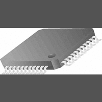
CLC021AVGZ-3.3 National Semiconductor, CLC021AVGZ-3.3 Datasheet - Page 15

CLC021AVGZ-3.3
Manufacturer Part Number
CLC021AVGZ-3.3
Description
IC, DIG VIDEO SERIALIZER, 3.63V, PQFP-44
Manufacturer
National Semiconductor
Datasheet
1.CLC021AVGZ-3.3.pdf
(18 pages)
Specifications of CLC021AVGZ-3.3
Ic Interface Type
Parallel, Serial
Supply Voltage Range
2.97V To 3.63V
Power Dissipation Pd
235mW
Operating Temperature Range
0°C To +70°C
Digital Ic Case Style
PQFP
No. Of Pins
44
Operating Temperature (min)
0C
Operating Temperature Classification
Commercial
Operating Temperature (max)
70C
Package Type
PQFP
Rad Hardened
No
Lead Free Status / RoHS Status
Contains lead / RoHS non-compliant
Lead Free Status / RoHS Status
Contains lead / RoHS non-compliant
Available stocks
Company
Part Number
Manufacturer
Quantity
Price
Company:
Part Number:
CLC021AVGZ-3.3
Manufacturer:
Texas Instruments
Quantity:
10 000
Part Number:
CLC021AVGZ-3.3
Manufacturer:
TI/德州仪器
Quantity:
20 000
Company:
Part Number:
CLC021AVGZ-3.3/NOPB
Manufacturer:
NSC
Quantity:
96
Company:
Part Number:
CLC021AVGZ-3.3/NOPB
Manufacturer:
Texas Instruments
Quantity:
10 000
Application Information
The Test Out output is intended for monitoring by equipment
having high impedance test loading (
Connect LOCK DETECT to TPG ENABLE for test pattern generator function.
Remove RP1 & RP3 and replace RP2 & RP4 with 50Ω resistor packs for coax interfacing.
Install RP1-4 when using ribbon cable for input interfacing.
This board is designed for use with TTL power supplies only.
MEASURING JITTER
The test method used to obtain the timing jitter value given in
the AC Electrical Specification table is based on procedures
and equipment described in SMPTE RP 192-1996. The rec-
ommended practice discusses several methods and indica-
tor devices. An FFT method performed by standard video
test equipment was used to obtain the data given in this data
sheet. As such, the jitter characteristics (or jitter floor) of the
measurement equipment, particularly the measurement ana-
lyzer, become integral to the resulting jitter value. The
>
500Ω). If the Lock
FIGURE 9. SD021EVK Schematic Diagram
(Continued)
15
Detect output is to be externally monitored, the attached
monitoring circuit should present a DC resistance greater
than 5 kΩ so as not to affect Lock Detect indicator operation.
method and equipment were chosen so that the test can be
easily duplicated by the design engineer using most stan-
dard digital video test equipment. In so doing, similar results
should be achieved. The intrinsic jitter floor of the CLC021’s
PLL is approximately 25% of the typical jitter given in the
electrical specifications. In production, device jitter is mea-
sured on automatic IC test equipment (ATE) using a different
method compatible with that equipment. Jitter measured
using this ATE yields values approximately 50% of those
obtained using the video test equipment.
10136809
www.national.com


