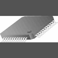
CLC021AVGZ-3.3 National Semiconductor, CLC021AVGZ-3.3 Datasheet - Page 14

CLC021AVGZ-3.3
Manufacturer Part Number
CLC021AVGZ-3.3
Description
IC, DIG VIDEO SERIALIZER, 3.63V, PQFP-44
Manufacturer
National Semiconductor
Datasheet
1.CLC021AVGZ-3.3.pdf
(18 pages)
Specifications of CLC021AVGZ-3.3
Ic Interface Type
Parallel, Serial
Supply Voltage Range
2.97V To 3.63V
Power Dissipation Pd
235mW
Operating Temperature Range
0°C To +70°C
Digital Ic Case Style
PQFP
No. Of Pins
44
Operating Temperature (min)
0C
Operating Temperature Classification
Commercial
Operating Temperature (max)
70C
Package Type
PQFP
Rad Hardened
No
Lead Free Status / RoHS Status
Contains lead / RoHS non-compliant
Lead Free Status / RoHS Status
Contains lead / RoHS non-compliant
Available stocks
Company
Part Number
Manufacturer
Quantity
Price
Company:
Part Number:
CLC021AVGZ-3.3
Manufacturer:
Texas Instruments
Quantity:
10 000
Part Number:
CLC021AVGZ-3.3
Manufacturer:
TI/德州仪器
Quantity:
20 000
Company:
Part Number:
CLC021AVGZ-3.3/NOPB
Manufacturer:
NSC
Quantity:
96
Company:
Part Number:
CLC021AVGZ-3.3/NOPB
Manufacturer:
Texas Instruments
Quantity:
10 000
www.national.com
Application Information
A typical application circuit for the CLC021 is shown in
Figure 8. This circuit demonstrates the capabilities of the
CLC021 and allows its evaluation in a variety of configura-
tions. Assembled demonstration boards with more compre-
hensive evaluation options are available, part number
SD021-5EVK (5V device) or SD021-3EVK (3.3V device).
APPLICATION CIRCUIT
The SD021EVK application circuit boards, Figure 9, can
accommodate different input and output drive and loading
options. Pin headers are provided for input and control I/O
signal access. Install the appropriate value resistor packs,
220Ω at RP1 and RP3 and 330Ω at RP2 and RP4, for TTL
cabled interfaces before applying input signals. Install 51Ω
resistor packs at RP2 and RP4 for signal sources requiring
such loading. Remove any resistor packs at RP1 and RP3
when using 50Ω source loading.
The board’s outputs may be DC interfaced to PECL inputs by
first installing 124Ω resistors at R1B and R2B, changing R1A
and R2A to 187Ω and replacing C1 and C2 with short
circuits. The PECL inputs should be directly connected to J1
and J2 without cabling. If 75Ω cabling is used to connect the
CLC021 to the PECL inputs, the voltage dividers used on the
FIGURE 8. Typical Application Circuit
14
The boards may be ordered through any of National’s sales
offices. Complete circuit board layouts and schematics in-
cluding Gerber photoplot files, for the demonstration boards
are available on National’s WEB site in the application infor-
mation for this device. For latest information, please see:
www.national.com/appinfo/interface.
CLC021 outputs must be removed and re-installed on the
circuit board where the PECL device is mounted. This will
provide correct termination for the cable and biasing for both
the CLC021’s outputs and the PECL inputs. It is most impor-
tant to note that a 75Ω or equivalent DC loading (measured
with respect to the negative supply rail) must always be
installed at both of the CLC021’s SDO outputs to obtain
proper signal levels from device. When using 75Ω Thevenin-
equivalent load circuits, the DC bias applied to the SDO
outputs should not exceed +3V (+1.3V for CLC021AVGZ-
3.3) with respect to the negative supply rail. Serial output
levels should be reduced to 400 mV
3.4 kΩ. This may be done by removing the Output Level
shorting jumper on the post header.
p-p
by changing R
10136808
REF
to


