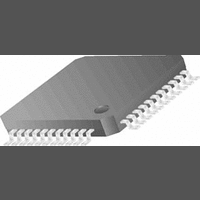
CLC021AVGZ-3.3 National Semiconductor, CLC021AVGZ-3.3 Datasheet - Page 16

CLC021AVGZ-3.3
Manufacturer Part Number
CLC021AVGZ-3.3
Description
IC, DIG VIDEO SERIALIZER, 3.63V, PQFP-44
Manufacturer
National Semiconductor
Datasheet
1.CLC021AVGZ-3.3.pdf
(18 pages)
Specifications of CLC021AVGZ-3.3
Ic Interface Type
Parallel, Serial
Supply Voltage Range
2.97V To 3.63V
Power Dissipation Pd
235mW
Operating Temperature Range
0°C To +70°C
Digital Ic Case Style
PQFP
No. Of Pins
44
Operating Temperature (min)
0C
Operating Temperature Classification
Commercial
Operating Temperature (max)
70C
Package Type
PQFP
Rad Hardened
No
Lead Free Status / RoHS Status
Contains lead / RoHS non-compliant
Lead Free Status / RoHS Status
Contains lead / RoHS non-compliant
Available stocks
Company
Part Number
Manufacturer
Quantity
Price
Company:
Part Number:
CLC021AVGZ-3.3
Manufacturer:
Texas Instruments
Quantity:
10 000
Part Number:
CLC021AVGZ-3.3
Manufacturer:
TI/德州仪器
Quantity:
20 000
Company:
Part Number:
CLC021AVGZ-3.3/NOPB
Manufacturer:
NSC
Quantity:
96
Company:
Part Number:
CLC021AVGZ-3.3/NOPB
Manufacturer:
Texas Instruments
Quantity:
10 000
www.national.com
Application Information
The jitter test setup used to obtain values quoted in the data
sheet consists of:
Apply the black-burst reference clock from the TG2000 sig-
nal generator’s BG1 module 27 MHz clock output to the level
converter input. The clock amplitude converter schematic is
shown in Figure 11. Adjust the input bias control to give a
50% duty cycle output as measured on the oscilloscope/
probe system. Connect the level translator to the SD021EVK
board, connector P1, P
• National Semiconductor SD021-5EVK (SD021-3EVK),
• Tektronix TG2000 signal generation platform with DVG1
• Tektronix VM700T Option 1S Video Measurement Set
• Tektronix TDS 794D, Option C2 oscilloscope
• Tektronix P6339A passive probe
• 75Ω coaxial cable, 3 ft., Belden 8281 or RG59 (2 re-
• ECL-to-TTL/CMOS
CLC021 evaluation kit
option
quired)
Figure 11).
CLK
level
pins (the outer-most row of pins
converter/amplifier,
FIGURE 11. ECL-to-TTL/CMOS Level Converter/Amplifer
(Continued)
FIGURE 10. Jitter Test Circuit
(see
16
is ground). Configure the SD021EVK to operate in the NTSC
colour bars, BIST mode. Configure the VM700T to make the
jitter measurement in the jitter FFT mode at the frame rate
with 1 kHz filter bandwidth and Hanning window. Configure
the setup as shown in Figure 10. Switch the test equipment
on (from standby mode) and allow all equipment tempera-
tures stabilize per manufacturer’s recommendation. Mea-
sure the jitter value after allowing the instrument’s reading to
stabilize (about 1 minute). Consult the VM700T Video Mea-
surement Set Option 1S Serial Digital Measurements User
Manual (document number 071-0074-00) for details of
equipment operation.
The VM700T measurement system’s jitter floor specification
at 270 Mbps is given as 200 ps
of actual components from 50 Hz to 1 MHz and 200 ps
+60%, -30% of actual components from 1 MHz to 10 MHz.
To obtain the actual residual jitter of the CLC021, a root-sum-
square adjustment of the jitter reading must be made to
compensate for the measurement system’s jitter floor speci-
fication. For example, if the jitter reading is 250 ps, the
CLC021 residual jitter is the square root of (250
150 ps. The accuracy limits of the reading as given above
apply.
±
20% (100 ps
10136813
±
2
5% typical)
10136810
− 200
2
) =


