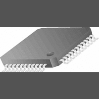
CLC021AVGZ-3.3 National Semiconductor, CLC021AVGZ-3.3 Datasheet

CLC021AVGZ-3.3
Specifications of CLC021AVGZ-3.3
Available stocks
Related parts for CLC021AVGZ-3.3
CLC021AVGZ-3.3 Summary of contents
Page 1
... VCO and the serializer improve power supply rejection, output jitter and noise performance. The CLC021AVGZ-5.0V is powered by a single +5V supply. The CLC021AVGZ-3.3V is powered by a single +3.3V sup- ply. Power dissipation is typically 235 mW including two 75Ω back-matched output loads. The device is packaged in a JEDEC metric 44-lead PQFP ...
Page 2
Block Diagram www.national.com 2 10136801 ...
Page 3
... Connection Diagram Order Number CLC021AVGZ-5.0 or CLC021AVGZ-3.3 44-Pin Metric PQFP See NS Package Number VGZ44A 3 10136802 www.national.com ...
Page 4
... CMOS Output Voltage OL Low Level V Serial Driver Output SDO Voltage I Power Supply Current, DD Total DC Electrical Characteristics—CLC021AVGZ-3.3 Over Supply Voltage and Operating Temperature ranges, unless otherwise specified (Notes 2, 3). Symbol Parameter V Input Voltage High Level IH V Input Voltage Low Level IL I Input Current High Level ...
Page 5
... Hold Time Figure 3 (Note 4) HLD L Output Inductance (Note 4) GEN R Output Resistance (Note 4) GEN AC Electrical Characteristics—CLC021AVGZ-3.3 Over Supply Voltage and Operating Temperature ranges, unless otherwise specified (Note 3). Symbol Parameter BR Serial Data Rate (Note 5) SDO Reference Clock F P CLK Input Frequency Reference Clock Duty ...
Page 6
... Note 2: Current flow into device pins is defined as positive. Current flow out of device pins is defined as negative. All voltages are stated referenced to V Note 3: Typical values are stated for V = +5.0V (CLC021AVGZ-5.0) or +3.3V (CLC021AVGZ-3.3) and T DD Note 4: Specification is guaranteed by design. ...
Page 7
Test Loads (Continued) FIGURE 2. Test Circuit 7 10136804 www.national.com ...
Page 8
Timing Diagram Device Operation The CLC021 SMPTE 259M Serial Digital Video Serializer is used in digital video signal origination equipment: cameras, video tape recorders, telecines and video test and other equipment. It converts parallel component or composite digi- tal video ...
Page 9
Device Operation (Continued) NRZ-TO-NRZI CONVERTER The NRZ-to-NRZI converter accepts NRZ serial data from the SMPTE and EDH polynomial genertors and converts it to NRZI using the polynomial ( per SMPTE 259M, para- graph 5.2 and Annex C. The ...
Page 10
Device Operation (Continued) FIGURE 5. Power-On Reset Sequence with Manual Reset BUILT-IN SELF-TEST (BIST) The CLC021 has a built-in self-test (BIST) function. The BIST performs a comprehensive go/no-go test of the device. The test uses either a full-field colour bar ...
Page 11
Device Operation (Continued) FIGURE 6. Built-In Self-Test Control Sequence TEST PATTERN GENERATOR The CLC021 includes an on-board test pattern generator (TPG). Four full-field component video test patterns for both NTSC and PAL standards, and 4x3 and 16x9 raster sizes are ...
Page 12
Device Operation (Continued) TABLE 1. BIST and Test Pattern Generator Control Functions Standard Frame NTSC 4x3 Flat-Field Black NTSC 4x3 PLL Pathological NTSC 4x3 EQ Pathological NTSC 4x3 Colour Bars, 75%, 8-Bars (modified, see text), BIST PAL 4x3 Flat-Field Black ...
Page 13
Pin Descriptions Pin Name 1 Reset 2 NRZ-NRZI 3 Test Out EDH Force 9 EDH Enable 10 SMPTE Mode 11 N ...
Page 14
... CLC021’s SDO outputs to obtain proper signal levels from device. When using 75Ω Thevenin- equivalent load circuits, the DC bias applied to the SDO outputs should not exceed +3V (+1.3V for CLC021AVGZ- 3.3) with respect to the negative supply rail. Serial output levels should be reduced to 400 mV 3.4 kΩ ...
Page 15
Application Information The Test Out output is intended for monitoring by equipment having high impedance test loading ( Connect LOCK DETECT to TPG ENABLE for test pattern generator function. Remove RP1 & RP3 and replace RP2 & RP4 with 50Ω ...
Page 16
... Application Information The jitter test setup used to obtain values quoted in the data sheet consists of: • National Semiconductor SD021-5EVK (SD021-3EVK), CLC021 evaluation kit • Tektronix TG2000 signal generation platform with DVG1 option • Tektronix VM700T Option 1S Video Measurement Set • Tektronix TDS 794D, Option C2 oscilloscope • ...
Page 17
Application Information PCB LAYOUT AND POWER SYSTEM BYPASS RECOMMENDATIONS Circuit board layout and stack-up for the CLC021 should be designed to provide noise-free power to the device. Good layout practice also will separate high frequency or high level inputs and ...
Page 18
... Physical Dimensions Order Number CLC021AVGZ-5.0 or CLC21AVGZ-3.3 LIFE SUPPORT POLICY NATIONAL’S PRODUCTS ARE NOT AUTHORIZED FOR USE AS CRITICAL COMPONENTS IN LIFE SUPPORT DEVICES OR SYSTEMS WITHOUT THE EXPRESS WRITTEN APPROVAL OF THE PRESIDENT AND GENERAL COUNSEL OF NATIONAL SEMICONDUCTOR CORPORATION. As used herein: 1. Life support devices or systems are devices or ...


