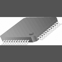
CLC021AVGZ-3.3 National Semiconductor, CLC021AVGZ-3.3 Datasheet - Page 4

CLC021AVGZ-3.3
Manufacturer Part Number
CLC021AVGZ-3.3
Description
IC, DIG VIDEO SERIALIZER, 3.63V, PQFP-44
Manufacturer
National Semiconductor
Datasheet
1.CLC021AVGZ-3.3.pdf
(18 pages)
Specifications of CLC021AVGZ-3.3
Ic Interface Type
Parallel, Serial
Supply Voltage Range
2.97V To 3.63V
Power Dissipation Pd
235mW
Operating Temperature Range
0°C To +70°C
Digital Ic Case Style
PQFP
No. Of Pins
44
Operating Temperature (min)
0C
Operating Temperature Classification
Commercial
Operating Temperature (max)
70C
Package Type
PQFP
Rad Hardened
No
Lead Free Status / RoHS Status
Contains lead / RoHS non-compliant
Lead Free Status / RoHS Status
Contains lead / RoHS non-compliant
Available stocks
Company
Part Number
Manufacturer
Quantity
Price
Company:
Part Number:
CLC021AVGZ-3.3
Manufacturer:
Texas Instruments
Quantity:
10 000
Part Number:
CLC021AVGZ-3.3
Manufacturer:
TI/德州仪器
Quantity:
20 000
Company:
Part Number:
CLC021AVGZ-3.3/NOPB
Manufacturer:
NSC
Quantity:
96
Company:
Part Number:
CLC021AVGZ-3.3/NOPB
Manufacturer:
Texas Instruments
Quantity:
10 000
www.national.com
V
V
I
I
V
V
V
I
V
V
I
I
IH
IL
DD
IH
IL
Symbol
Symbol
IH
IL
OH
OL
SDO
IH
IL
Absolute Maximum Ratings
is anticipated that this device will not be offered in a
military qualified version. If Military/Aerospace speci-
fied devices are required, please contact the National
Semiconductor Sales Office / Distributors for availabil-
ity and specifications.
DC Electrical Characteristics—CLC021AVGZ-5.0
Over Supply Voltage and Operating Temperature ranges, unless otherwise specified (Notes 2, 3).
DC Electrical Characteristics—CLC021AVGZ-3.3
Over Supply Voltage and Operating Temperature ranges, unless otherwise specified (Notes 2, 3).
Supply Voltage (V
CMOS/TTL Input Voltage (V
CMOS/TTL Output Voltage (V
CMOS/TTL Input Current (single input):
Input Current, Other Inputs:
CMOS/TTL Output Source/Sink Current:
SDO Output Source Current:
Package Thermal Resistance
CLC021AVGZ-5.0V
CLC021AVGZ-3.3V
CLC021AVGZ-5.0V
CLC021AVGZ-3.3V
CLC021AVGZ-5.0V
CLC021AVGZ-3.3V
V
V
θ
JA
I
I
(
(
= V
= V
@
@
44-lead Metric PQFP:
0 LFM airflow)
500 LFM airflow)
SS
DD
Input Voltage High Level
Input Voltage Low Level
Input Current High Level
Input Current Low Level
CMOS Output Voltage
High Level
CMOS Output Voltage
Low Level
Serial Driver Output
Voltage
Power Supply Current,
Total
Input Voltage High Level
Input Voltage Low Level
Input Current High Level
Input Current Low Level
−0.5V:
+0.5V:
Parameter
Parameter
DD
−V
SS
):
I
):
O
):
V
V
I
I
R
R
Figure 2
R
R
P
Colour Bar Pattern,
Figure 2
V
V
OH
OL
IH
IL
L
REF
L
REF
CLK
IH
IL
−0.5V to V
−0.5V to V
-0.3V to V
-0.3V to V
= 75Ω 1%,
= 75Ω 1%,
= V
= +10 mA
= V
= V
= −10 mA
= V
= 27 MHz, NTSC
= 1.69 kΩ 1%,
= 1.69 kΩ 1%,
SS
SS
DD
DD
Conditions
Conditions
(Note 1) It
DD
DD
DD
DD
±
60˚C/W
43˚C/W
±
−5 mA
+5 mA
16 mA
22 mA
+0.5V
+0.3V
+0.5V
+0.3V
1 mA
6.0V
4.0V
4
Recommended Operating
Conditions
Storage Temp. Range:
Junction Temperature:
Lead Temperature (Soldering 4
Sec):
ESD Rating (HBM):
ESD Rating (MM):
Transistor Count:
Supply Voltage (V
CMOS/TTL Input Voltage:
Maximum DC Bias on SDO pins:
P
P
D
Operating Free Air Temperature
(T
All CMOS Inputs
All CMOS
Outputs
SDO, SDO
All CMOS Inputs
CLK
CLK
N
A
θ
CLC021AVGZ-5.0
CLC021AVGZ-3.3
CLC021AVGZ-5.0
CLC021AVGZ-3.3
):
JC
Reference
Reference
and P
Frequency Range
Duty Cycle
44-lead Metric PQFP:
CLK
Rise/Fall Time
DD
−V
Min
V
700
Min
V
2.0
2.4
0.0
2.0
SS
SS
SS
):
Typ
Typ
+40
800
+22
4.7
0.3
47
-1
-1
V
SS
Max
Max
V
V
V
+60
900
+60
-20
-20
0.8
0.6
60
−65˚C to +150˚C
+ 0.5V
DD
DD
DD
0˚C to +70˚C
10 to 40MHz
1.0 to 3.0 ns
5.0V
3.3V
3.0V
1.3V
V
45 to 55%
SS
17˚C/W
+150˚C
+260˚C
33,400
to V
±
±
±
±
mV
150V
Units
Units
2 kV
10%
10%
10%
10%
mA
µA
µA
µA
µA
V
V
V
V
V
V
DD
P-P


