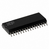
CLRC63201T/0FE,112 NXP Semiconductors, CLRC63201T/0FE,112 Datasheet - Page 6

CLRC63201T/0FE,112
Manufacturer Part Number
CLRC63201T/0FE,112
Description
IC I.CODE HS READER 32-SOIC
Manufacturer
NXP Semiconductors
Series
I-Coder
Specifications of CLRC63201T/0FE,112
Rf Type
Read Only
Frequency
13.56MHz
Features
ISO14443-A, ISO14443-B, ISO15693, ISO18000-3
Package / Case
32-SOIC (0.300", 7.50mm Width)
Product
RFID Readers
Operating Temperature Range
- 25 C to + 85 C
Lead Free Status / RoHS Status
Lead free / RoHS Compliant
Lead Free Status / RoHS Status
Lead free / RoHS Compliant, Lead free / RoHS Compliant
Other names
568-2199-5
935269690112
CLRC632
CLRC63201TD
935269690112
CLRC632
CLRC63201TD
Available stocks
Company
Part Number
Manufacturer
Quantity
Price
Company:
Part Number:
CLRC63201T/0FE,112
Manufacturer:
IR
Quantity:
3 400
Part Number:
CLRC63201T/0FE,112
Manufacturer:
NXP/恩智浦
Quantity:
20 000
NXP Semiconductors
Table 3.
[1]
[2]
[3]
CLRC632_35
Product data sheet
PUBLIC
Pin
11
12
13
13 to 20
21
22
23
24
25
26
27
28
29
30
31
32
[3]
[3]
[3]
[3]
Pin types: I = Input, O = Output, I/O = Input/Output, P = Power and G = Ground.
The SLRC400 uses pin name SIGOUT for pin MFOUT. The CLRC632 functionality includes test functions for the SLRC400 using pin
MFOUT.
These pins provide different functionality depending on the selected microprocessor interface type (see
detailed information).
[3]
Pin description
Symbol
NRD
NDS
nDStrb
DVSS
D0
D0 to D7
AD0 to AD7
ALE
AS
nAStrb
NSS
A0
nWait
MOSI
A1
A2
SCK
DVDD
AVDD
AUX
AVSS
RX
VMID
RSTPD
OSCOUT
…continued
Type
I
I
I
G
O
I/O
I/O
I
I
I
I
I
O
I
I
I
I
P
P
O
G
I
P
I
O
[1]
Description
not read input generates the strobe signal for reading data from the CLRC632
registers when applied to pins D0 to D7
not data strobe input generates the strobe signal for the read and write cycles
not data strobe input generates the strobe signal for the read and write cycles
digital ground
SPI master in, slave out output
8-bit bidirectional data bus input/output on pins D0 to D7
8-bit bidirectional address and data bus input/output on pins AD0 to AD7
address latch enable input for pins AD0 to AD5; HIGH latches the internal address
address strobe input for pins AD0 to AD5; HIGH latches the internal address
not address strobe input for pins AD0 to AD5; LOW latches the internal address
not slave select strobe input for SPI communication
address line 0 is the address register bit 0 input
not wait output:
SPI master out, slave in
address line 1 is the address register bit 1 input
address line 2 is the address register bit 2 input
SPI serial clock input
digital power supply
analog power supply for pins OSCIN, OSCOUT, RX, VMID and AUX
auxiliary output is used to generate analog test signals. The output signal is
selected using the TestAnaSelect register’s TestAnaOutSel[4:0] bits
analog ground
receiver input is used as the card response input. The carrier is load modulated at
13.56 MHz, drawn from the antenna circuit
internal reference voltage pin provides the internal reference voltage as a supply
Remark: It must be connected to a 100 nF block capacitor connected between pin
VMID and ground
reset and power-down input:
crystal oscillator output for the oscillator’s inverting amplifier
LOW starts an access cycle
HIGH ends an access cycle
HIGH: the internal current sinks are switched off, the oscillator is inhibited and
the input pads are disconnected
LOW (negative edge): start internal reset phase
Rev. 3.5 — 10 November 2009
Multiple protocol contactless reader IC (MIFARE/I-CODE1)
073935
Section 9.1 on page 7
CLRC632
© NXP B.V. 2009. All rights reserved.
for
6 of 126


