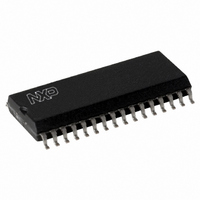
CLRC63201T/0FE,112 NXP Semiconductors, CLRC63201T/0FE,112 Datasheet - Page 101

CLRC63201T/0FE,112
Manufacturer Part Number
CLRC63201T/0FE,112
Description
IC I.CODE HS READER 32-SOIC
Manufacturer
NXP Semiconductors
Series
I-Coder
Specifications of CLRC63201T/0FE,112
Rf Type
Read Only
Frequency
13.56MHz
Features
ISO14443-A, ISO14443-B, ISO15693, ISO18000-3
Package / Case
32-SOIC (0.300", 7.50mm Width)
Product
RFID Readers
Operating Temperature Range
- 25 C to + 85 C
Lead Free Status / RoHS Status
Lead free / RoHS Compliant
Lead Free Status / RoHS Status
Lead free / RoHS Compliant, Lead free / RoHS Compliant
Other names
568-2199-5
935269690112
CLRC632
CLRC63201TD
935269690112
CLRC632
CLRC63201TD
Available stocks
Company
Part Number
Manufacturer
Quantity
Price
Company:
Part Number:
CLRC63201T/0FE,112
Manufacturer:
IR
Quantity:
3 400
Part Number:
CLRC63201T/0FE,112
Manufacturer:
NXP/恩智浦
Quantity:
20 000
NXP Semiconductors
CLRC632_35
Product data sheet
PUBLIC
13.3.2 Digital output pin characteristics
13.3.3 Antenna driver output pin characteristics
Pin RSTPD has Schmitt trigger CMOS characteristics. In addition, it is internally filtered by
a RC low-pass filter which causes a propagation delay on the reset signal.
Table 164. RSTPD input pin characteristics
The analog input pin RX has the input capacitance and input voltage range shown in
Table
Table 165. RX input capacitance and input voltage range
Pins D0 to D7, MFOUT and IRQ have CMOS output characteristics and behave as
defined in
Table 166. Digital output pin characteristics
Remark: Pin IRQ can be configured as open collector which causes the V
no longer applicable.
The source conductance of the antenna driver pins TX1 and TX2 for driving the
HIGH-level can be configured using the CwConductance register’s GsCfgCW[5:0] bits,
while their source conductance for driving the LOW-level is constant.
The antenna driver default configuration output characteristics are specified in
Symbol Parameter
I
V
t
Symbol
C
V
Symbol
V
V
I
LI
PD
O
th
i(dyn)
OH
OL
i
165.
input leakage current
threshold voltage
propagation delay
Table
Parameter
voltage
LOW-level output
voltage
output current
HIGH-level output
Parameter
input capacitance
dynamic input voltage
166.
Rev. 3.5 — 10 November 2009
Multiple protocol contactless reader IC (MIFARE/I-CODE1)
073935
Conditions
positive-going threshold;
CMOS = V
negative-going threshold;
CMOS = V
Conditions
V
Conditions
V
V
V
V
source or sink; V
DDA
DDD
DDD
DDD
DDD
= 5 V; T
= 5 V; I
= 5 V; I
= 5 V; I
= 5 V; I
DDD
DDD
< 3.6 V
< 3.6 V
amb
OH
OH
OL
OL
= 1 mA
= 10 mA
= 1 mA
= 10 mA
= 25 C
DDD
= 5 V
Min
0.65V
0.25V
-
1.0
DDD
DDD
Min
-
1.1
Min
2.4
2.4
-
-
-
Typ Max
-
-
-
-
CLRC632
Typ
-
-
© NXP B.V. 2009. All rights reserved.
Typ
4.9
4.2
25
250
-
OH
+1.0
0.75V
0.4V
20
Max
15
4.4
values to be
Max
-
-
400
400
10
DDD
Table
DDD
101 of 126
Unit
pF
V
Unit
V
V
mV
mV
mA
Unit
V
V
167.
A
s


