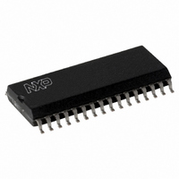
CLRC63201T/0FE,112 NXP Semiconductors, CLRC63201T/0FE,112 Datasheet - Page 35

CLRC63201T/0FE,112
Manufacturer Part Number
CLRC63201T/0FE,112
Description
IC I.CODE HS READER 32-SOIC
Manufacturer
NXP Semiconductors
Series
I-Coder
Specifications of CLRC63201T/0FE,112
Rf Type
Read Only
Frequency
13.56MHz
Features
ISO14443-A, ISO14443-B, ISO15693, ISO18000-3
Package / Case
32-SOIC (0.300", 7.50mm Width)
Product
RFID Readers
Operating Temperature Range
- 25 C to + 85 C
Lead Free Status / RoHS Status
Lead free / RoHS Compliant
Lead Free Status / RoHS Status
Lead free / RoHS Compliant, Lead free / RoHS Compliant
Other names
568-2199-5
935269690112
CLRC632
CLRC63201TD
935269690112
CLRC632
CLRC63201TD
Available stocks
Company
Part Number
Manufacturer
Quantity
Price
Company:
Part Number:
CLRC63201T/0FE,112
Manufacturer:
IR
Quantity:
3 400
Part Number:
CLRC63201T/0FE,112
Manufacturer:
NXP/恩智浦
Quantity:
20 000
NXP Semiconductors
CLRC632_35
Product data sheet
PUBLIC
Fig 12. Receiver circuit block diagram
RX
ClkQDelay[4:0]
9.10.2.1 Automatic Q-clock calibration
DEMODULATOR
9.10.1 Receiver circuit block diagram
9.10.2 Receiver operation
CONVERSION
I-clock
13.56 MHz
I TO Q
ClkQCalib
The quadrature demodulator uses two different clocks (Q-clock and I-clock) with a
phase-shift of 90 between them. Both resulting subcarrier signals are amplified, filtered
and forwarded to the correlation circuitry. The correlation results are evaluated, digitized
and then passed to the digital circuitry. Various adjustments can be made to obtain
optimum performance for all processing units.
Figure 12
broken down in to several steps. Quadrature demodulation of the 13.56 MHz carrier signal
is performed. To achieve the optimum performance, automatic Q-clock calibration is
recommended (see
The demodulated signal is amplified by an adjustable amplifier. A correlation circuit
calculates the degree of similarity between the expected and the received signal. The
BitPhase register enables correlation interval position alignment with the received signal’s
bit grid. In the evaluation and digitizer circuitry, the valid bits are detected and the digital
results are sent to the FIFO buffer. Several tuning steps are possible for this circuit.
The signal can be observed on its way through the receiver as shown in
signal at a time can be routed to pin AUX using the TestAnaSelect register as described in
Section 15.2.2 on page
In general, the default settings programmed in the StartUp initialization file are suitable for
use with the CLRC632 to MIFARE card data communication. However, in some
environments specific user settings will achieve better performance.
The quadrature demodulation concept of the receiver generates a phase signal (I-clock)
and a 90 phase-shifted quadrature signal (Q-clock). To achieve the optimum demodulator
performance, the Q-clock and the I-clock must be phase-shifted by 90 . After the reset
phase, a calibration procedure is automatically performed.
Q-clock
VRxFollI
ClkQ180Deg
clock
VRxFollQ
shows the block diagram of the receiver circuit. The receiving process can be
Gain[1:0]
VRxAmpI
Section 9.10.2.1 on page
VRxAmpQ
Rev. 3.5 — 10 November 2009
112.
CORRELATION
Multiple protocol contactless reader IC (MIFARE/I-CODE1)
BitPhase[7:0]
CIRCUITRY
073935
TestAnaOutSel
to
VCorrDI
VCorrNI
35).
VCorrDQ
VCorrNQ
MinLevel[3:0]
CollLevel[3:0]
VEvalR
EVALUATION
CIRCUITRY
DIGITIZER
AND
RxWait[7:0]
VEvalL
RcvClkSell
CLRC632
© NXP B.V. 2009. All rights reserved.
Figure
001aak615
s_valid
s_data
s_coll
s_clock
12. One
35 of 126


