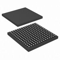
HSP50216KIZ Intersil, HSP50216KIZ Datasheet - Page 45

HSP50216KIZ
Manufacturer Part Number
HSP50216KIZ
Description
IC DOWNCONVERTER DGTL 4CH 196BGA
Manufacturer
Intersil
Datasheet
1.HSP50216KIZ.pdf
(58 pages)
Specifications of HSP50216KIZ
Function
Downconverter
Rf Type
W-CDMA
Package / Case
196-BGA
Lead Free Status / RoHS Status
Lead free / RoHS Compliant
P(31:0)
P(15:0)
P(15:0)
P(15:0)
P(15:0)
31:22
19:18
17:16
15:0
15:0
N/A
N/A
N/A
21
20
Set to zero.
1
0
1
0
This bit may also be set low temporarily when free running to stabilize the accumulator data for reading.
Input Level Detector Leak factor, A.
00
01
10
11
Input Level Detector Mode
00
01
10
Input Level Detector Interval
Load with two less than the desired number of input samples. The interval range is 2 to 65537 input samples.
Writing to this location clears the input level detector accumulator and restarts the interval counter. When the interval counter is done,
bit 1 of the status word is set.
This 16-bit value can be used as the input to one or more NCO/Mixer/CIC sections or to the input level detector for test or to set the
input to a constant value to minimize power when the channel is not in use.
The ENI signal for this input is either bit 11 in the channel register at IWA *000h or the strobe generated by a write to location GWA
F808h (selected via bit 12 of the channel register at IWA *000h).
A write to this location, generates and ENI strobe for the μP driven input port (when selected via bit 12 of IWA *000h).
A write to this location will cause a one-clock-wide pulse on the SYNCO pin. The SYNCO pin is used to synchronize multiple channels
or parts. The SYNCO pin from one part is typically connected to the SYNCI pin of all the parts. Up to two pipeline registers may be
inserted in the SYNCO to SYNCI path.
Rectify input samples. Ones complement the 16-bit data after formatting if the value is negative.
Unmodified input.
Free run (ignore interval counter).
Stop when interval counter times out.
1
2
2
2
Leaky integrator (Y
Peak detector.
Integrator (bit 20 should be set to 0).
-8
-12
-16
TABLE 40. INPUT LEVEL DETECTOR CONFIGURATION REGISTER (GWA = F805h)
TABLE 41. INPUT LEVEL DETECTOR START STROBE REGISTER (GWA = F806h)
45
TABLE 43. μP/TEST INPUT BUS ENI REGISTER (GWA = F808h)
n
TABLE 42. μP/TEST INPUT BUS REGISTER (GWA = F807h)
= A*X
TABLE 44. SYNCO STROBE REGISTER (GWA = F809h)
n
+ (1-A)*Y
n-1
, where A is the gain selected in bits 19:18).
HSP50216
FUNCTION
FUNCTION
FUNCTION
FUNCTION
FUNCTION
August 17, 2007
FN4557.6


