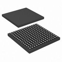
HSP50216KIZ Intersil, HSP50216KIZ Datasheet - Page 34

HSP50216KIZ
Manufacturer Part Number
HSP50216KIZ
Description
IC DOWNCONVERTER DGTL 4CH 196BGA
Manufacturer
Intersil
Datasheet
1.HSP50216KIZ.pdf
(58 pages)
Specifications of HSP50216KIZ
Function
Downconverter
Rf Type
W-CDMA
Package / Case
196-BGA
Lead Free Status / RoHS Status
Lead free / RoHS Compliant
31:0 for RD
N/A for WR
P(31:0)
P(31:0)
P(15:0)
P(31:0)
P(31:0)
P(31:0)
P(31:0)
31:0
31:0
31:8
N/A
2:1
7:0
31
30
29
0
Number of Carrier Offset Frequency (COF) serial input bits. The format is 2’s complement, early SYNC, MSB first:
00
01
10
11
Enable serial carrier offset frequency (zeros the data already loaded via the COF/COFSYNC pins). To disable the COF shifting see
IWA register *000h.
Carrier Center Frequency (CCF):
This is the frequency control for the carrier NCO. The center frequency control is double buffered. The contents of this register are
transferred to the active register on a write to the CCFStrobe location or on a SYNCI (if load on SYNCI is enabled). The carrier center
frequency is: CCF*f
CCF is a twos complement number and has a range of -2
mode and the clock rate for interpolated mode.
Writing to this address generates a strobe that transfers the CCF value to the active frequency register. The transfer to the active
register can also be done using the SYNCI pin to synchronize the transfer in multiple parts or to synchronize to an external event.
The value in the active register can be read at this address (the center frequency control before the serially loaded offset value is
added). To read the value, either write this address to A(1:0) = 11 and then read at A(1:0) = 00 and 01, or read the value at A(1:0) =
00 and 01 after writing to this address and before writing a new address to either A(1:0) = 10 or 11.
These are the upper 32 bits of the 56-bit timing (resampler) NCO center frequency control.
These are the lower 24 bits of the 56-bit timing (resampler) NCO center frequency control.
Unused, set to zero.
A write to this location will update the resampler NCO center frequency. The upper 32 bits of the active register can be read at this
address.
μPHold. When set, this bit stops the filter compute engine and allows the μP access to the instruction and coefficient RAMs for
reading and writing. On the high to low transition, the filter compute engine is reset (the read and write pointers are reset and the
instruction at location 31 is fetched).
μPShiftZeroB. This bit, when set to zero, disables the coefficient shift bits (bits 9:8 of the master register when coefficient loading).
μPEN Limit. This bit disables the data path saturation logic. Provided for test. Active high. Set to 0 to disable the normal ROM
controlled limiting (ANDed with normal signal).
TABLE 9. CARRIER NCO CENTER FREQUENCY UPDATE STROBE REGISTER (IWA = *006h)
TABLE 13. FILTER COMPUTE ENGINE/RESAMPLER CONTROL REGISTER (IWA = *00Ah)
TABLE 12. TIMING NCO CENTER FREQUENCY LOAD STROBE REGISTER (IWA = *009h)
8
16
24
32
TABLE 10. TIMING NCO FREQUENCY CONTROL REGISTER, MSW (IWA = *007h)
TABLE 11. TIMING NCO FREQUENCY CONTROL REGISTER, LSW (IWA = *008h)
TABLE 7. CARRIER NCO/CIC CONTROL REGISTER (IWA = *004h) (Continued)
34
TABLE 8. CARRIER NCO CENTER FREQUENCY REGISTER (IWA = *005h)
CLK
/(2
32
).
HSP50216
31
FUNCTION
FUNCTION
FUNCTION
FUNCTION
FUNCTION
FUNCTION
FUNCTION
to (2
31
-1). f
CLK
is the input sample rate (ENIx assertion rate) for gated
August 17, 2007
FN4557.6


