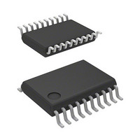
R5F21294SNSP#U0 Renesas Electronics America, R5F21294SNSP#U0 Datasheet - Page 340

R5F21294SNSP#U0
Manufacturer Part Number
R5F21294SNSP#U0
Description
MCU 3/5V 16K+2K 20PIN-SSOP
Manufacturer
Renesas Electronics America
Series
M16C™ M16C/R8C/Tiny/29r
Datasheet
1.R5F21282SNSPU0.pdf
(473 pages)
Specifications of R5F21294SNSP#U0
Core Processor
R8C
Core Size
16-Bit
Speed
20MHz
Connectivity
I²C, LIN, SIO, SSU, UART/USART
Peripherals
LED, POR, Voltage Detect, WDT
Number Of I /o
13
Program Memory Size
16KB (16K x 8)
Program Memory Type
FLASH
Ram Size
1K x 8
Voltage - Supply (vcc/vdd)
2.2 V ~ 5.5 V
Data Converters
A/D 4x10b
Oscillator Type
Internal
Operating Temperature
-20°C ~ 85°C
Package / Case
20-SSOP
Lead Free Status / RoHS Status
Lead free / RoHS Compliant
Eeprom Size
-
Available stocks
Company
Part Number
Manufacturer
Quantity
Price
- Current page: 340 of 473
- Download datasheet (5Mb)
R8C/28 Group, R8C/29 Group
Rev.2.10
REJ09B0279-0210
Figure 17.8
Timer RA Set the pulse width measurement level low
Timer RA Set the count source (f1, f2, f8, fOCO)
Timer RA Set the Synch Break width
Hardware LIN Set the LIN operation to stop
Hardware LIN Set to slave mode
Hardware LIN Set the LIN operation to start
Hardware LIN Set the RXD0 input unmasking timing
Hardware LIN Set the register to enable interrupts
Timer RA Set to pulse width measurement mode
Timer RA Set the INT1/TRAIO pin to P1_5
Sep 26, 2008
Bits TCK0 to TCK2 in the TRAMR register
TRAPRE register
TRA register
TEDGSEL bit in the TRAIOC register ← 0
Bits TMOD0 to TMOD2 in the TRAMR register ← 011b
TIOSEL bit in the TRAIOC register ← 1
LINE bit in the LINCR register ← 1
Example of Header Field Reception Flowchart (1)
(After Synch Break detection, or after Synch
Field measurement)
SBE bit in the LINCR register
(Bus collision detection, Synch Break detection,
Synch Field measurement)
Bits BCIE, SBIE, SFIE in the LINCR register
MST bit in the LINCR register ← 0
LINE bit in the LINCR register ← 0
Page 321 of 441
A
For the hardware LIN
function, set the TIOSEL bit
in the TRAIOC register to 1.
Set the count source and registers
TRA and TRAPRE as appropriate
for the Synch Break period.
Select the timing at which to
unmask the RXD0 input for UART0.
If the RXD0 input is chosen to be
unmasked after detection of Synch
Break, the Synch Field signal is
also input to UART0.
17. Hardware LIN
Related parts for R5F21294SNSP#U0
Image
Part Number
Description
Manufacturer
Datasheet
Request
R

Part Number:
Description:
KIT STARTER FOR M16C/29
Manufacturer:
Renesas Electronics America
Datasheet:

Part Number:
Description:
KIT STARTER FOR R8C/2D
Manufacturer:
Renesas Electronics America
Datasheet:

Part Number:
Description:
R0K33062P STARTER KIT
Manufacturer:
Renesas Electronics America
Datasheet:

Part Number:
Description:
KIT STARTER FOR R8C/23 E8A
Manufacturer:
Renesas Electronics America
Datasheet:

Part Number:
Description:
KIT STARTER FOR R8C/25
Manufacturer:
Renesas Electronics America
Datasheet:

Part Number:
Description:
KIT STARTER H8S2456 SHARPE DSPLY
Manufacturer:
Renesas Electronics America
Datasheet:

Part Number:
Description:
KIT STARTER FOR R8C38C
Manufacturer:
Renesas Electronics America
Datasheet:

Part Number:
Description:
KIT STARTER FOR R8C35C
Manufacturer:
Renesas Electronics America
Datasheet:

Part Number:
Description:
KIT STARTER FOR R8CL3AC+LCD APPS
Manufacturer:
Renesas Electronics America
Datasheet:

Part Number:
Description:
KIT STARTER FOR RX610
Manufacturer:
Renesas Electronics America
Datasheet:

Part Number:
Description:
KIT STARTER FOR R32C/118
Manufacturer:
Renesas Electronics America
Datasheet:

Part Number:
Description:
KIT DEV RSK-R8C/26-29
Manufacturer:
Renesas Electronics America
Datasheet:

Part Number:
Description:
KIT STARTER FOR SH7124
Manufacturer:
Renesas Electronics America
Datasheet:

Part Number:
Description:
KIT STARTER FOR H8SX/1622
Manufacturer:
Renesas Electronics America
Datasheet:

Part Number:
Description:
KIT DEV FOR SH7203
Manufacturer:
Renesas Electronics America
Datasheet:


