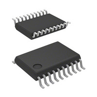
R5F21294SNSP#U0 Renesas Electronics America, R5F21294SNSP#U0 Datasheet - Page 326

R5F21294SNSP#U0
Manufacturer Part Number
R5F21294SNSP#U0
Description
MCU 3/5V 16K+2K 20PIN-SSOP
Manufacturer
Renesas Electronics America
Series
M16C™ M16C/R8C/Tiny/29r
Datasheet
1.R5F21282SNSPU0.pdf
(473 pages)
Specifications of R5F21294SNSP#U0
Core Processor
R8C
Core Size
16-Bit
Speed
20MHz
Connectivity
I²C, LIN, SIO, SSU, UART/USART
Peripherals
LED, POR, Voltage Detect, WDT
Number Of I /o
13
Program Memory Size
16KB (16K x 8)
Program Memory Type
FLASH
Ram Size
1K x 8
Voltage - Supply (vcc/vdd)
2.2 V ~ 5.5 V
Data Converters
A/D 4x10b
Oscillator Type
Internal
Operating Temperature
-20°C ~ 85°C
Package / Case
20-SSOP
Lead Free Status / RoHS Status
Lead free / RoHS Compliant
Eeprom Size
-
Available stocks
Company
Part Number
Manufacturer
Quantity
Price
- Current page: 326 of 473
- Download datasheet (5Mb)
R8C/28 Group, R8C/29 Group
Rev.2.10
REJ09B0279-0210
Figure 16.44
16.3.6
Table 16.8
1Tcyc = 1/f1(s)
When setting the I
two cases:
Therefore, the SCL signal is monitored and communication is synchronized bit by bit.
Figure 16.44 shows the Timing of Bit Synchronization Circuit and Table 16.8 lists the Time between Changing
SCL Signal from “L” Output to High-Impedance and Monitoring of SCL Signal.
• If the SCL signal is driven L level by a slave device
• If the rise speed of the SCL signal is reduced by a load (load capacity or pull-up resistor) on the SCL line.
Sep 26, 2008
Bit Synchronization Circuit
CKS3
0
1
Timing of Bit Synchronization Circuit
Monitoring of SCL Signal
Time between Changing SCL Signal from “L” Output to High-Impedance and
ICCR1 Register
SCL monitor timing
Reference clock of
2
C bus interface to master mode, the high-level period may become shorter in the following
Page 307 of 441
Internal SCL
SCL
CKS2
0
1
0
1
VIH
7.5Tcyc
19.5Tcyc
17.5Tcyc
41.5Tcyc
Time for Monitoring SCL
16. Clock Synchronous Serial Interface
Related parts for R5F21294SNSP#U0
Image
Part Number
Description
Manufacturer
Datasheet
Request
R

Part Number:
Description:
KIT STARTER FOR M16C/29
Manufacturer:
Renesas Electronics America
Datasheet:

Part Number:
Description:
KIT STARTER FOR R8C/2D
Manufacturer:
Renesas Electronics America
Datasheet:

Part Number:
Description:
R0K33062P STARTER KIT
Manufacturer:
Renesas Electronics America
Datasheet:

Part Number:
Description:
KIT STARTER FOR R8C/23 E8A
Manufacturer:
Renesas Electronics America
Datasheet:

Part Number:
Description:
KIT STARTER FOR R8C/25
Manufacturer:
Renesas Electronics America
Datasheet:

Part Number:
Description:
KIT STARTER H8S2456 SHARPE DSPLY
Manufacturer:
Renesas Electronics America
Datasheet:

Part Number:
Description:
KIT STARTER FOR R8C38C
Manufacturer:
Renesas Electronics America
Datasheet:

Part Number:
Description:
KIT STARTER FOR R8C35C
Manufacturer:
Renesas Electronics America
Datasheet:

Part Number:
Description:
KIT STARTER FOR R8CL3AC+LCD APPS
Manufacturer:
Renesas Electronics America
Datasheet:

Part Number:
Description:
KIT STARTER FOR RX610
Manufacturer:
Renesas Electronics America
Datasheet:

Part Number:
Description:
KIT STARTER FOR R32C/118
Manufacturer:
Renesas Electronics America
Datasheet:

Part Number:
Description:
KIT DEV RSK-R8C/26-29
Manufacturer:
Renesas Electronics America
Datasheet:

Part Number:
Description:
KIT STARTER FOR SH7124
Manufacturer:
Renesas Electronics America
Datasheet:

Part Number:
Description:
KIT STARTER FOR H8SX/1622
Manufacturer:
Renesas Electronics America
Datasheet:

Part Number:
Description:
KIT DEV FOR SH7203
Manufacturer:
Renesas Electronics America
Datasheet:


