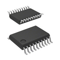
R5F21294SNSP#U0 Renesas Electronics America, R5F21294SNSP#U0 Datasheet - Page 149

R5F21294SNSP#U0
Manufacturer Part Number
R5F21294SNSP#U0
Description
MCU 3/5V 16K+2K 20PIN-SSOP
Manufacturer
Renesas Electronics America
Series
M16C™ M16C/R8C/Tiny/29r
Datasheet
1.R5F21282SNSPU0.pdf
(473 pages)
Specifications of R5F21294SNSP#U0
Core Processor
R8C
Core Size
16-Bit
Speed
20MHz
Connectivity
I²C, LIN, SIO, SSU, UART/USART
Peripherals
LED, POR, Voltage Detect, WDT
Number Of I /o
13
Program Memory Size
16KB (16K x 8)
Program Memory Type
FLASH
Ram Size
1K x 8
Voltage - Supply (vcc/vdd)
2.2 V ~ 5.5 V
Data Converters
A/D 4x10b
Oscillator Type
Internal
Operating Temperature
-20°C ~ 85°C
Package / Case
20-SSOP
Lead Free Status / RoHS Status
Lead free / RoHS Compliant
Eeprom Size
-
Available stocks
Company
Part Number
Manufacturer
Quantity
Price
- Current page: 149 of 473
- Download datasheet (5Mb)
R8C/28 Group, R8C/29 Group
Rev.2.10
REJ09B0279-0210
Figure 13.2
Watchdog Timer Control Register
Option Function Select Register
b7 b6 b5 b4
b7 b6 b5 b4
NOTES:
1.
2.
3.
4.
5.
6.
0 0
The OFS register is on the flash memory. Write to the OFS register w ith a program. After w riting is completed, do not
w rite additions to the OFS register.
The LVD0ON bit setting is valid only by a hardw are reset. To use the pow er-on reset, set the LVD0ON bit to 0
(voltage monitor 0 reset enabled after hardw are reset).
If the block including the OFS register is erased, FFh is set to the OFS register.
For N, D version only. For J, K version, set the LVD0ON bit to 1 (voltage monitor 0 reset disabled after hardw are
reset).
The LVD1ON bit setting is valid only by a hardw are reset. When the pow er-on reset function is used, set the
LVD1ON bit to 0 (voltage monitor 1 reset enabled after hardw are reset).
For J, K version only. For N, D version, set the LVD1ON bit to 1 (voltage monitor 1 reset disabled after hardw are
reset).
Sep 26, 2008
1
b3 b2 b1 b0
b3 b2 b1 b0
Registers OFS and WDC
1
Bit Symbol
Bit Symbol
CSPROINI
ROMCP1
LVD0ON
LVD1ON
WDTON
ROMCR
(b4-b0)
Symbol
Symbol
WDC7
WDC
OFS
(b1)
(b4)
(b5)
(b6)
Page 130 of 441
—
—
—
—
—
High-order bits of w atchdog timer
Reserved bit
Reserved bit
Prescaler select bit
Watchdog timer start
select bit
Reserved bit
ROM code protect
disabled bit
ROM code protect bit
Reserved bit
Voltage detection 0
circuit start bit
Voltage detection 1
circuit start bit
Count source protect
mode after reset select
bit
(1)
Address
Bit Name
Address
Bit Name
0FFFFh
000Fh
(2, 4)
(5, 6)
Set to 0. When read, the content is undefined.
Set to 0.
0 : Divide-by-16
1 : Divide-by-128
0 : Starts w atchdog timer automatically after reset
1 : Watchdog timer is inactive after reset
Set to 1.
0 : ROM code protect disabled
1 : ROMCP1 enabled
0 : ROM code protect enabled
1 : ROM code protect disabled
Set to 1.
0 : Voltage monitor 0 reset enabled after hardw are
1 : Voltage monitor 0 reset disabled after hardw are
0 : Voltage monitor 1 reset enabled after hardw are
1 : Voltage monitor 1 reset disabled after hardw are
0 : Count source protect mode enabled after reset
1 : Count source protect mode disabled after reset
reset
reset
reset
reset
When Shipping
After Reset
00X11111b
Function
Function
FFh
(3)
13. Watchdog Timer
RW
RW
RW
RW
RW
RW
RW
RW
RW
RW
RW
RW
RW
RO
Related parts for R5F21294SNSP#U0
Image
Part Number
Description
Manufacturer
Datasheet
Request
R

Part Number:
Description:
KIT STARTER FOR M16C/29
Manufacturer:
Renesas Electronics America
Datasheet:

Part Number:
Description:
KIT STARTER FOR R8C/2D
Manufacturer:
Renesas Electronics America
Datasheet:

Part Number:
Description:
R0K33062P STARTER KIT
Manufacturer:
Renesas Electronics America
Datasheet:

Part Number:
Description:
KIT STARTER FOR R8C/23 E8A
Manufacturer:
Renesas Electronics America
Datasheet:

Part Number:
Description:
KIT STARTER FOR R8C/25
Manufacturer:
Renesas Electronics America
Datasheet:

Part Number:
Description:
KIT STARTER H8S2456 SHARPE DSPLY
Manufacturer:
Renesas Electronics America
Datasheet:

Part Number:
Description:
KIT STARTER FOR R8C38C
Manufacturer:
Renesas Electronics America
Datasheet:

Part Number:
Description:
KIT STARTER FOR R8C35C
Manufacturer:
Renesas Electronics America
Datasheet:

Part Number:
Description:
KIT STARTER FOR R8CL3AC+LCD APPS
Manufacturer:
Renesas Electronics America
Datasheet:

Part Number:
Description:
KIT STARTER FOR RX610
Manufacturer:
Renesas Electronics America
Datasheet:

Part Number:
Description:
KIT STARTER FOR R32C/118
Manufacturer:
Renesas Electronics America
Datasheet:

Part Number:
Description:
KIT DEV RSK-R8C/26-29
Manufacturer:
Renesas Electronics America
Datasheet:

Part Number:
Description:
KIT STARTER FOR SH7124
Manufacturer:
Renesas Electronics America
Datasheet:

Part Number:
Description:
KIT STARTER FOR H8SX/1622
Manufacturer:
Renesas Electronics America
Datasheet:

Part Number:
Description:
KIT DEV FOR SH7203
Manufacturer:
Renesas Electronics America
Datasheet:


