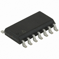
ATTINY24-15SSZ Atmel, ATTINY24-15SSZ Datasheet - Page 74

ATTINY24-15SSZ
Manufacturer Part Number
ATTINY24-15SSZ
Description
MCU AVR 2K FLASH 15MHZ 14-SOIC
Manufacturer
Atmel
Series
AVR® ATtinyr
Datasheet
1.ATTINY24-15SSZ.pdf
(225 pages)
Specifications of ATTINY24-15SSZ
Package / Case
14-SOIC (3.9mm Width), 14-SOL
Voltage - Supply (vcc/vdd)
2.7 V ~ 5.5 V
Operating Temperature
-40°C ~ 125°C
Speed
16MHz
Number Of I /o
12
Eeprom Size
128 x 8
Core Processor
AVR
Program Memory Type
FLASH
Ram Size
128 x 8
Program Memory Size
2KB (2K x 8)
Data Converters
A/D 8x10b
Oscillator Type
Internal
Peripherals
Brown-out Detect/Reset, POR, PWM, WDT
Connectivity
USI
Core Size
8-Bit
Cpu Family
ATtiny
Device Core
AVR
Device Core Size
8b
Frequency (max)
16MHz
Interface Type
SPI/UART
Total Internal Ram Size
128Byte
# I/os (max)
12
Number Of Timers - General Purpose
2
Operating Supply Voltage (typ)
3.3/5V
Operating Supply Voltage (max)
5.5V
Operating Supply Voltage (min)
2.7V
On-chip Adc
8-chx10-bit
Instruction Set Architecture
RISC
Operating Temp Range
-40C to 125C
Operating Temperature Classification
Automotive
Mounting
Surface Mount
Pin Count
14
Package Type
SOIC
Lead Free Status / RoHS Status
Lead free / RoHS Compliant
Available stocks
Company
Part Number
Manufacturer
Quantity
Price
Company:
Part Number:
ATTINY24-15SSZ
Manufacturer:
ATMEL
Quantity:
349
Part Number:
ATTINY24-15SSZ
Manufacturer:
ATTINY
Quantity:
20 000
- Current page: 74 of 225
- Download datasheet (4Mb)
13.5.1
13.5.2
74
Atmel ATtiny24/44/84 [Preliminary]
Force Output Compare
Compare Match Blocking by TCNT0 Write
Figure 13-3. Output Compare Unit, Block Diagram
The OCR0x registers are double buffered when using any of the pulse width modulation
(PWM) modes. For the normal and clear timer on compare (CTC) modes of operation, the
double buffering is disabled. The double buffering synchronizes the update of the OCR0x
compare registers to either top or bottom of the counting sequence. The synchronization pre-
vents the occurrence of odd-length, non-symmetrical PWM pulses, thereby making the output
glitch-free.
The OCR0x register access may seem complex, but this is not the case. When the double
buffering is enabled, the CPU has access to the OCR0x buffer register, and if double buffering
is disabled the CPU will access the OCR0x directly.
In non-PWM waveform generation modes, the match output of the comparator can be forced
by writing a logical one to the force output compare (0x) bit. Forcing compare match will not
set the OCF0x flag or reload/clear the timer, but the OC0x pin will be updated as if a real com-
pare match had occurred (the COM0x1:0 bits settings define whether the OC0x pin is set,
cleared, or toggled).
All CPU write operations to the TCNT0 Register will block any Compare Match that occur in
the next timer clock cycle, even when the timer is stopped. This feature allows OCR0x to be
initialized to the same value as TCNT0 without triggering an interrupt when the Timer/Counter
clock is enabled.
bottom
FOCn
top
OCRnx
Waveform Generator
WGMn1:0
=
(8-bit Comparator )
DATA BUS
COMnX1:0
TCNTn
OCFnx (Int.Req.)
OCnx
7701D–AVR–09/10
Related parts for ATTINY24-15SSZ
Image
Part Number
Description
Manufacturer
Datasheet
Request
R

Part Number:
Description:
Manufacturer:
Atmel Corporation
Datasheet:

Part Number:
Description:
Manufacturer:
Atmel Corporation
Datasheet:

Part Number:
Description:
IC MCU AVR 2K FLASH 20MHZ 20-QFN
Manufacturer:
Atmel
Datasheet:

Part Number:
Description:
IC MCU AVR 2K FLASH 20MHZ 14SOIC
Manufacturer:
Atmel
Datasheet:

Part Number:
Description:
MCU AVR 2K FLASH 15MHZ 20-QFN
Manufacturer:
Atmel
Datasheet:

Part Number:
Description:
IC MCU AVR 2K FLASH 20MHZ 14-DIP
Manufacturer:
Atmel
Datasheet:

Part Number:
Description:
MCU AVR 2KB FLASH 20MHZ 14SOIC
Manufacturer:
Atmel
Datasheet:

Part Number:
Description:
MCU AVR 2KB FLASH 20MHZ 20QFN
Manufacturer:
Atmel
Datasheet:

Part Number:
Description:
IC, MCU, 8BIT, 2K FLASH, 20SOIC
Manufacturer:
Atmel
Datasheet:

Part Number:
Description:
IC, MCU, 8BIT, 2K FLASH, 20PDIP
Manufacturer:
Atmel
Datasheet:

Part Number:
Description:
IC, MCU, 8BIT, 8K FLASH, 20PDIP
Manufacturer:
Atmel
Datasheet:

Part Number:
Description:
IC, MCU, 8BIT, 8K FLASH, 20SOIC
Manufacturer:
Atmel
Datasheet:


