ATTINY24-15SSZ Atmel, ATTINY24-15SSZ Datasheet - Page 140
ATTINY24-15SSZ
Manufacturer Part Number
ATTINY24-15SSZ
Description
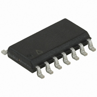
MCU AVR 2K FLASH 15MHZ 14-SOIC
Manufacturer
Atmel
Series
AVR® ATtinyr
Datasheet
1.ATTINY24-15SSZ.pdf
(225 pages)
Specifications of ATTINY24-15SSZ
Package / Case
14-SOIC (3.9mm Width), 14-SOL
Voltage - Supply (vcc/vdd)
2.7 V ~ 5.5 V
Operating Temperature
-40°C ~ 125°C
Speed
16MHz
Number Of I /o
12
Eeprom Size
128 x 8
Core Processor
AVR
Program Memory Type
FLASH
Ram Size
128 x 8
Program Memory Size
2KB (2K x 8)
Data Converters
A/D 8x10b
Oscillator Type
Internal
Peripherals
Brown-out Detect/Reset, POR, PWM, WDT
Connectivity
USI
Core Size
8-Bit
Cpu Family
ATtiny
Device Core
AVR
Device Core Size
8b
Frequency (max)
16MHz
Interface Type
SPI/UART
Total Internal Ram Size
128Byte
# I/os (max)
12
Number Of Timers - General Purpose
2
Operating Supply Voltage (typ)
3.3/5V
Operating Supply Voltage (max)
5.5V
Operating Supply Voltage (min)
2.7V
On-chip Adc
8-chx10-bit
Instruction Set Architecture
RISC
Operating Temp Range
-40C to 125C
Operating Temperature Classification
Automotive
Mounting
Surface Mount
Pin Count
14
Package Type
SOIC
Lead Free Status / RoHS Status
Lead free / RoHS Compliant
Available stocks
Company
Part Number
Manufacturer
Quantity
Price
Company:

Part Number:
ATTINY24-15SSZ
Manufacturer:
ATMEL
Quantity:
349
Part Number:
ATTINY24-15SSZ
Manufacturer:
ATTINY
Quantity:
20 000


140
Atmel ATtiny24/44/84 [Preliminary]
The prescaling is set by the ADPS bits in ADCSRA. The prescaler starts counting from the
moment the ADC is switched on by setting the ADEN bit in ADCSRA. The prescaler keeps
running for as long as the ADEN bit is set, and is continuously reset when ADEN is low.
When initiating a single-ended conversion by setting the ADSC bit in ADCSRA, the conversion
starts at the following rising edge of the ADC clock cycle.
A normal conversion takes 13 ADC clock cycles. The first conversion after the ADC is
switched on (ADEN in ADCSRA is set) takes 25 ADC clock cycles in order to initialize the ana-
log circuitry.
The actual sample-and-hold takes place 1.5 ADC clock cycles after the start of a normal con-
version and 14.5 ADC clock cycles after the start of a first conversion. When a conversion is
complete, the result is written to the ADC data registers, and ADIF is set. In single-conversion
mode, ADSC is cleared simultaneously. The software may then set ADSC again, and a new
conversion will be initiated on the first rising ADC clock edge.
When auto triggering is used, the prescaler is reset when the trigger event occurs. This
assures a fixed delay from the trigger event to the start of conversion. In this mode, the sam-
ple-and-hold takes place two ADC clock cycles after the rising edge on the trigger source
signal. Three additional CPU clock cycles are used for synchronization logic.
In free running mode, a new conversion will be started immediately after the conversion com-
pletes, while ADSC remains high. For a summary of conversion times, see
page
Figure 18-4. ADC Timing Diagram, First Conversion (Single Conversion Mode)
Figure 18-5. ADC Timing Diagram, Single Conversion
Cycle Number
ADC Clock
ADSC
ADIF
ADCH
ADCL
Cycle Number
ADC Clock
ADEN
ADSC
ADIF
ADCH
ADCL
141.
1
1
2
MUX and REFS
Update
2
MUX and REFS
Update
12
3
13
Sample & Hold
4
14
5
15
6
Sample & Hold
16
First Conversion
17
7
One Conversion
18
8
19
9
20
10
Conversion
Complete
21
11
22
Conversion
Complete
23
12
24
13
25
Sign and MSB of Result
Sign and MSB of Result
LSB of Result
Next Conversion
1
Next
Conversion
1
LSB of Result
Table 18-1 on
2
7701D–AVR–09/10
2
MUX and REFS
Update
MUX and REFS
Update
3
3
Related parts for ATTINY24-15SSZ
Image
Part Number
Description
Manufacturer
Datasheet
Request
R

Part Number:
Description:
Manufacturer:
Atmel Corporation
Datasheet:
Part Number:
Description:
Manufacturer:
Atmel Corporation
Datasheet:

Part Number:
Description:
IC MCU AVR 2K FLASH 20MHZ 20-QFN
Manufacturer:
Atmel
Datasheet:

Part Number:
Description:
IC MCU AVR 2K FLASH 20MHZ 14SOIC
Manufacturer:
Atmel
Datasheet:

Part Number:
Description:
MCU AVR 2K FLASH 15MHZ 20-QFN
Manufacturer:
Atmel
Datasheet:

Part Number:
Description:
IC MCU AVR 2K FLASH 20MHZ 14-DIP
Manufacturer:
Atmel
Datasheet:

Part Number:
Description:
MCU AVR 2KB FLASH 20MHZ 14SOIC
Manufacturer:
Atmel
Datasheet:
Part Number:
Description:
MCU AVR 2KB FLASH 20MHZ 20QFN
Manufacturer:
Atmel
Datasheet:
Part Number:
Description:
IC, MCU, 8BIT, 2K FLASH, 20SOIC
Manufacturer:
Atmel
Datasheet:

Part Number:
Description:
IC, MCU, 8BIT, 2K FLASH, 20PDIP
Manufacturer:
Atmel
Datasheet:
Part Number:
Description:
IC, MCU, 8BIT, 8K FLASH, 20PDIP
Manufacturer:
Atmel
Datasheet:
Part Number:
Description:
IC, MCU, 8BIT, 8K FLASH, 20SOIC
Manufacturer:
Atmel
Datasheet: