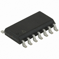
ATTINY24-15SSZ Atmel, ATTINY24-15SSZ Datasheet - Page 142

ATTINY24-15SSZ
Manufacturer Part Number
ATTINY24-15SSZ
Description
MCU AVR 2K FLASH 15MHZ 14-SOIC
Manufacturer
Atmel
Series
AVR® ATtinyr
Datasheet
1.ATTINY24-15SSZ.pdf
(225 pages)
Specifications of ATTINY24-15SSZ
Package / Case
14-SOIC (3.9mm Width), 14-SOL
Voltage - Supply (vcc/vdd)
2.7 V ~ 5.5 V
Operating Temperature
-40°C ~ 125°C
Speed
16MHz
Number Of I /o
12
Eeprom Size
128 x 8
Core Processor
AVR
Program Memory Type
FLASH
Ram Size
128 x 8
Program Memory Size
2KB (2K x 8)
Data Converters
A/D 8x10b
Oscillator Type
Internal
Peripherals
Brown-out Detect/Reset, POR, PWM, WDT
Connectivity
USI
Core Size
8-Bit
Cpu Family
ATtiny
Device Core
AVR
Device Core Size
8b
Frequency (max)
16MHz
Interface Type
SPI/UART
Total Internal Ram Size
128Byte
# I/os (max)
12
Number Of Timers - General Purpose
2
Operating Supply Voltage (typ)
3.3/5V
Operating Supply Voltage (max)
5.5V
Operating Supply Voltage (min)
2.7V
On-chip Adc
8-chx10-bit
Instruction Set Architecture
RISC
Operating Temp Range
-40C to 125C
Operating Temperature Classification
Automotive
Mounting
Surface Mount
Pin Count
14
Package Type
SOIC
Lead Free Status / RoHS Status
Lead free / RoHS Compliant
Available stocks
Company
Part Number
Manufacturer
Quantity
Price
Company:
Part Number:
ATTINY24-15SSZ
Manufacturer:
ATMEL
Quantity:
349
Part Number:
ATTINY24-15SSZ
Manufacturer:
ATTINY
Quantity:
20 000
18.6
18.6.1
18.6.2
142
Changing Channel or Reference Selection
Atmel ATtiny24/44/84 [Preliminary]
ADC Input Channels
ADC Voltage Reference
The MUX5:0 and REFS1:0 bits in the ADMUX register are single-buffered through a tempo-
rary register to which the CPU has random access. This ensures that the channel and
reference selection only takes place at a safe point during the conversion. The channel and
reference selection is continuously updated until a conversion is started. Once the conversion
starts, the channel and reference selection is locked to ensure a sufficient sampling time for
the ADC. Continuous updating resumes in the last ADC clock cycle before the conversion
completes (ADIF in ADCSRA is set). Note that the conversion starts on the following rising
ADC clock edge after ADSC is written. The user is thus advised not to write new channel or
reference selection values to ADMUX until one ADC clock cycle after ADSC is written.
If auto triggering is used, the exact time of the triggering event can be indeterministic. Special
care must be taken when updating the ADMUX register in order to control which conversion
will be affected by the new setting.
If both ADATE and ADEN are written to logical one, an interrupt event can occur at any time. If
the ADMUX register is changed in this period, the user cannot tell if the next conversion is
based on the old or the new setting. The ADMUX register can be safely updated in the follow-
ing ways:
When updating the ADMUX register in one of these conditions, the new setting will affect the
next ADC conversion.
When changing channel selections, the user should observe the following guidelines to ensure
that the correct channel is selected:
In single-conversion mode, always select the channel before starting the conversion. The
channel selection may be changed one ADC clock cycle after writing logical one to ADSC.
However, the simplest method is to wait for the conversion to complete before changing the
channel selection.
In free running mode, always select the channel before starting the first conversion. The chan-
nel selection may be changed one ADC clock cycle after writing logical one to ADSC.
However, the simplest method is to wait for the first conversion to complete, and then change
the channel selection. Because the next conversion has already started automatically, the
next result will reflect the previous channel selection. Subsequent conversions will reflect the
new channel selection.
The reference voltage for the ADC (V
gle-ended channels that exceed V
as either V
after switching the reference voltage source may be inaccurate, and the user is advised to dis-
card this result.
a. When ADATE or ADEN is cleared.
b. During conversion, minimum one ADC clock cycle after the trigger event.
c. After a conversion, before the Interrupt Flag used as the trigger source is cleared.
CC
, internal 1.1V reference, or external AREF pin. The first ADC conversion result
REF
will result in codes close to 0x3FF. V
REF
) indicates the conversion range for the ADC. Sin-
REF
can be selected
7701D–AVR–09/10


