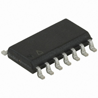
ATTINY24-15SSZ Atmel, ATTINY24-15SSZ Datasheet - Page 64

ATTINY24-15SSZ
Manufacturer Part Number
ATTINY24-15SSZ
Description
MCU AVR 2K FLASH 15MHZ 14-SOIC
Manufacturer
Atmel
Series
AVR® ATtinyr
Datasheet
1.ATTINY24-15SSZ.pdf
(225 pages)
Specifications of ATTINY24-15SSZ
Package / Case
14-SOIC (3.9mm Width), 14-SOL
Voltage - Supply (vcc/vdd)
2.7 V ~ 5.5 V
Operating Temperature
-40°C ~ 125°C
Speed
16MHz
Number Of I /o
12
Eeprom Size
128 x 8
Core Processor
AVR
Program Memory Type
FLASH
Ram Size
128 x 8
Program Memory Size
2KB (2K x 8)
Data Converters
A/D 8x10b
Oscillator Type
Internal
Peripherals
Brown-out Detect/Reset, POR, PWM, WDT
Connectivity
USI
Core Size
8-Bit
Cpu Family
ATtiny
Device Core
AVR
Device Core Size
8b
Frequency (max)
16MHz
Interface Type
SPI/UART
Total Internal Ram Size
128Byte
# I/os (max)
12
Number Of Timers - General Purpose
2
Operating Supply Voltage (typ)
3.3/5V
Operating Supply Voltage (max)
5.5V
Operating Supply Voltage (min)
2.7V
On-chip Adc
8-chx10-bit
Instruction Set Architecture
RISC
Operating Temp Range
-40C to 125C
Operating Temperature Classification
Automotive
Mounting
Surface Mount
Pin Count
14
Package Type
SOIC
Lead Free Status / RoHS Status
Lead free / RoHS Compliant
Available stocks
Company
Part Number
Manufacturer
Quantity
Price
Company:
Part Number:
ATTINY24-15SSZ
Manufacturer:
ATMEL
Quantity:
349
Part Number:
ATTINY24-15SSZ
Manufacturer:
ATTINY
Quantity:
20 000
- Current page: 64 of 225
- Download datasheet (4Mb)
64
Atmel ATtiny24/44/84 [Preliminary]
• Port A, Bit 1 – ADC1/AIN0/PCINT1
ADC1: Analog to Digital Converter, Channel 1
AIN0: Analog Comparator Positive Input. Configure the port pin as input with the internal
pull-up switched off to avoid the digital port function from interfering with the function of the
Analog Comparator.
PCINT1: Pin Change Interrupt source 1. The PA1 pin can serve as an external interrupt
source for pin change interrupt 0.
• Port A, Bit 2 – ADC2/AIN1/PCINT2
ADC2: Analog to Digital Converter, Channel 2
AIN1: Analog Comparator Negative Input. Configure the port pin as input with the internal
pull-up switched off to avoid the digital port function from interfering with the function of the
Analog Comparator.
PCINT2: Pin Change Interrupt source 2. The PA2 pin can serve as an external interrupt
source for pin change interrupt 0.
• Port A, Bit 3 – ADC3/T0/PCINT3
ADC3: Analog to digital converter, channel 3.
T0: Timer/counter 0 counter source.
PCINT3: Pin change interrupt source 3. The PA3 pin can serve as an external interrupt source
for pin change interrupt 0.
• Port A, Bit 4 – ADC4/USCK/SCL/T1/PCINT4
ADC4: Analog to Digital Converter, Channel 4
USCK: Three-wire mode Universal Serial Interface Clock.
SCL: Two-wire mode Serial Clock for USI Two-wire mode.
T1: Timer/Counter1 counter source.
PCINT4: Pin Change Interrupt source 4. The PA4 pin can serve as an external interrupt
source for pin change interrupt 0.
• Port A, Bit 5 – ADC5/DO/OC1B/PCINT5
ADC5: Analog to digital converter, channel 5.
DO: Data output in USI three-wire mode. Data output (DO) overrides PORTA5 value, and it is
driven to the port when the data direction bit DDA5 is set (one). However the PORTA5 bit still
controls the pull-up, enabling pull-up if direction is input and PORTA5 is set (one).
OC1B: Output compare match output: The PA5 pin can serve as an external output for the
Timer/Counter1 compare match B. The PA5 pin has to be configured as an output (DDA5 set
(one)) to serve this function. The OC1B pin is also the output pin for the PWM mode timer
function.
PCINT5: Pin change interrupt source 5. The PA5 pin can serve as an external interrupt source
for pin change interrupt 0.
.
.
.
7701D–AVR–09/10
Related parts for ATTINY24-15SSZ
Image
Part Number
Description
Manufacturer
Datasheet
Request
R

Part Number:
Description:
Manufacturer:
Atmel Corporation
Datasheet:

Part Number:
Description:
Manufacturer:
Atmel Corporation
Datasheet:

Part Number:
Description:
IC MCU AVR 2K FLASH 20MHZ 20-QFN
Manufacturer:
Atmel
Datasheet:

Part Number:
Description:
IC MCU AVR 2K FLASH 20MHZ 14SOIC
Manufacturer:
Atmel
Datasheet:

Part Number:
Description:
MCU AVR 2K FLASH 15MHZ 20-QFN
Manufacturer:
Atmel
Datasheet:

Part Number:
Description:
IC MCU AVR 2K FLASH 20MHZ 14-DIP
Manufacturer:
Atmel
Datasheet:

Part Number:
Description:
MCU AVR 2KB FLASH 20MHZ 14SOIC
Manufacturer:
Atmel
Datasheet:

Part Number:
Description:
MCU AVR 2KB FLASH 20MHZ 20QFN
Manufacturer:
Atmel
Datasheet:

Part Number:
Description:
IC, MCU, 8BIT, 2K FLASH, 20SOIC
Manufacturer:
Atmel
Datasheet:

Part Number:
Description:
IC, MCU, 8BIT, 2K FLASH, 20PDIP
Manufacturer:
Atmel
Datasheet:

Part Number:
Description:
IC, MCU, 8BIT, 8K FLASH, 20PDIP
Manufacturer:
Atmel
Datasheet:

Part Number:
Description:
IC, MCU, 8BIT, 8K FLASH, 20SOIC
Manufacturer:
Atmel
Datasheet:


