ATTINY24-15SSZ Atmel, ATTINY24-15SSZ Datasheet - Page 153
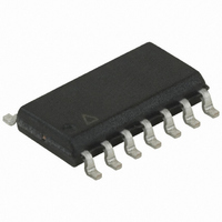
ATTINY24-15SSZ
Manufacturer Part Number
ATTINY24-15SSZ
Description
MCU AVR 2K FLASH 15MHZ 14-SOIC
Manufacturer
Atmel
Series
AVR® ATtinyr
Datasheet
1.ATTINY24-15SSZ.pdf
(225 pages)
Specifications of ATTINY24-15SSZ
Package / Case
14-SOIC (3.9mm Width), 14-SOL
Voltage - Supply (vcc/vdd)
2.7 V ~ 5.5 V
Operating Temperature
-40°C ~ 125°C
Speed
16MHz
Number Of I /o
12
Eeprom Size
128 x 8
Core Processor
AVR
Program Memory Type
FLASH
Ram Size
128 x 8
Program Memory Size
2KB (2K x 8)
Data Converters
A/D 8x10b
Oscillator Type
Internal
Peripherals
Brown-out Detect/Reset, POR, PWM, WDT
Connectivity
USI
Core Size
8-Bit
Cpu Family
ATtiny
Device Core
AVR
Device Core Size
8b
Frequency (max)
16MHz
Interface Type
SPI/UART
Total Internal Ram Size
128Byte
# I/os (max)
12
Number Of Timers - General Purpose
2
Operating Supply Voltage (typ)
3.3/5V
Operating Supply Voltage (max)
5.5V
Operating Supply Voltage (min)
2.7V
On-chip Adc
8-chx10-bit
Instruction Set Architecture
RISC
Operating Temp Range
-40C to 125C
Operating Temperature Classification
Automotive
Mounting
Surface Mount
Pin Count
14
Package Type
SOIC
Lead Free Status / RoHS Status
Lead free / RoHS Compliant
Available stocks
Company
Part Number
Manufacturer
Quantity
Price
Company:

Part Number:
ATTINY24-15SSZ
Manufacturer:
ATMEL
Quantity:
349
Part Number:
ATTINY24-15SSZ
Manufacturer:
ATTINY
Quantity:
20 000


18.10.4
7701D–AVR–09/10
ADCSRB – ADC Control and Status Register B
• Bits 7 – BIN: Bipolar Input Mode
The gain stage is working in the unipolar mode by default, but the bipolar mode can be
selected by writing the BIN bit in the ADCSRB register. In the unipolar mode, only one-sided
conversions are supported, and the voltage on the positive input must always be larger than
the voltage on the negative input. Otherwise, the result is saturated to the voltage reference. In
the bipolar mode, two-sided conversions are supported, and the result is represented in two's
complement form. In unipolar mode, the resolution is 10 bits, and in bipolar mode the resolu-
tion is 9 bits + 1 sign bit.
• Bit 6 – ACME: Analog Comparator Multiplexer Enable
See
• Bit 5 – Res: Reserved Bit
This bit is reserved bit in the Atmel® ATtiny24/44/84, and will always read as what was written
there.
• Bit 4 – ADLAR: ADC Left Adjust Result
The ADLAR bit affects the presentation of the ADC conversion result in the ADC data register.
Write logical one to ADLAR to left adjust the result. Otherwise, the result is right adjusted.
Changing the ADLAR bit will affect the ADC data register immediately, regardless of any
ongoing conversions. For a complete description of this bit, see
Data Register” on page
• Bit 3 – Res: Reserved Bit
This bit is reserved bit in the Atmel
there.
• Bits 2:0 – ADTS2:0: ADC Auto Trigger Source
If ADATE in ADCSRA is written to logical one, the value of these bits selects which source will
trigger an ADC conversion. If ADATE is cleared, the ADTS2:0 settings will have no effect. A
conversion will be triggered by the rising edge of the selected interrupt flag. Note that switch-
ing from a trigger source that is cleared to a trigger source that is set will generate a positive
edge on the trigger signal. If ADEN in ADCSRA is set, this will start a conversion. Switching to
free running mode (ADTS[2:0]=0) will not cause a trigger event, even if the ADC Interrupt Flag
is set.
Bit
0x03 (0x23)
Read/Write
Initial Value
“ADCSRB – ADC Control and Status Register B” on page
R/W
BIN
7
0
152.
ACME
R/W
6
0
Atmel ATtiny24/44/84 [Preliminary]
R/W
®
5
–
0
ATtiny24/44/84, and will always read as what was written
ADLAR
R/W
4
0
R/W
3
–
0
ADTS2
R/W
2
0
134.
“ADCL and ADCH – ADC
ADTS1
R/W
1
0
ADTS0
R/W
0
0
ADCSRB
153
Related parts for ATTINY24-15SSZ
Image
Part Number
Description
Manufacturer
Datasheet
Request
R

Part Number:
Description:
Manufacturer:
Atmel Corporation
Datasheet:
Part Number:
Description:
Manufacturer:
Atmel Corporation
Datasheet:

Part Number:
Description:
IC MCU AVR 2K FLASH 20MHZ 20-QFN
Manufacturer:
Atmel
Datasheet:

Part Number:
Description:
IC MCU AVR 2K FLASH 20MHZ 14SOIC
Manufacturer:
Atmel
Datasheet:

Part Number:
Description:
MCU AVR 2K FLASH 15MHZ 20-QFN
Manufacturer:
Atmel
Datasheet:

Part Number:
Description:
IC MCU AVR 2K FLASH 20MHZ 14-DIP
Manufacturer:
Atmel
Datasheet:

Part Number:
Description:
MCU AVR 2KB FLASH 20MHZ 14SOIC
Manufacturer:
Atmel
Datasheet:
Part Number:
Description:
MCU AVR 2KB FLASH 20MHZ 20QFN
Manufacturer:
Atmel
Datasheet:
Part Number:
Description:
IC, MCU, 8BIT, 2K FLASH, 20SOIC
Manufacturer:
Atmel
Datasheet:

Part Number:
Description:
IC, MCU, 8BIT, 2K FLASH, 20PDIP
Manufacturer:
Atmel
Datasheet:
Part Number:
Description:
IC, MCU, 8BIT, 8K FLASH, 20PDIP
Manufacturer:
Atmel
Datasheet:
Part Number:
Description:
IC, MCU, 8BIT, 8K FLASH, 20SOIC
Manufacturer:
Atmel
Datasheet: