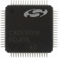
C8051F018-GQ Silicon Laboratories Inc, C8051F018-GQ Datasheet - Page 91

C8051F018-GQ
Manufacturer Part Number
C8051F018-GQ
Description
IC 8051 MCU 16K FLASH 64TQFP
Manufacturer
Silicon Laboratories Inc
Series
C8051F018r
Specifications of C8051F018-GQ
Program Memory Type
FLASH
Program Memory Size
16KB (16K x 8)
Package / Case
64-TQFP, 64-VQFP
Core Processor
8051
Core Size
8-Bit
Speed
25MHz
Connectivity
SMBus (2-Wire/I²C), SPI, UART/USART
Peripherals
Brown-out Detect/Reset, POR, PWM, Temp Sensor, WDT
Number Of I /o
32
Ram Size
1.25K x 8
Voltage - Supply (vcc/vdd)
2.8 V ~ 3.6 V
Data Converters
A/D 8x10b
Oscillator Type
Internal
Operating Temperature
-40°C ~ 85°C
Processor Series
C8051F0x
Core
8051
Data Bus Width
8 bit
Data Ram Size
1.25 KB
Interface Type
I2C/SMBus/SPI/UART
Maximum Clock Frequency
25 MHz
Number Of Programmable I/os
32
Number Of Timers
4
Operating Supply Voltage
2.8 V to 3.6 V
Maximum Operating Temperature
+ 85 C
Mounting Style
SMD/SMT
3rd Party Development Tools
PK51, CA51, A51, ULINK2
Development Tools By Supplier
C8051F005DK
Minimum Operating Temperature
- 40 C
On-chip Adc
8-ch x 10-bit
Lead Free Status / RoHS Status
Lead free / RoHS Compliant
Eeprom Size
-
Lead Free Status / Rohs Status
Lead free / RoHS Compliant
Other names
336-1197
Available stocks
Company
Part Number
Manufacturer
Quantity
Price
Company:
Part Number:
C8051F018-GQ
Manufacturer:
SiliconL
Quantity:
39
Company:
Part Number:
C8051F018-GQ
Manufacturer:
Silicon Laboratories Inc
Quantity:
10 000
Company:
Part Number:
C8051F018-GQR
Manufacturer:
Silicon Laboratories Inc
Quantity:
10 000
91
WEAKPUD
Bit7:
Bit6:
Bits5-1: UNUSED. Read = 00000b, Write = don’t care.
Bit0:
Example Usage of XBR0, XBR1, XBR2:
When selected, the digital resources fill the Port I/O pins in order (top to bottom as shown in
The MCUs have a wide array of digital resources, which are available through four digital I/O
ports, P0, P1, P2 and P3. Each of the pins on Ports 0, 1, and 2 can be defined as either its
corresponding port I/O or one of the internal digital resources assigned as shown in Figure 13.1.
The designer has complete control over which functions are assigned, limited only by the
number of physical I/O pins available on the selected package (the C8051F018 has all four ports
pinned out, and the C8051F019 has P0 and P1). This resource assignment flexibility is achieved
through the use of a Priority CrossBar Decoder. (Note that the state of a Port I/O pin can always
be read in the corresponding Port latch regardless of the Crossbar settings).
The CrossBar assigns the selected internal digital resources to the I/O pins based on the Priority
C8051F018
C8051F019
R/W
Bit7
0: Weak Pull-ups Enabled (except for Ports whose I/O are configured as push-pull)
1: Weak Pull-ups Disabled
0: Crossbar Disabled
1: Crossbar Enabled
CNVSTE: ADC Convert Start Input Enable Bit
0: CNVSTR unavailable at Port pin.
1: CNVSTR routed to Port Pin.
WEAKPUD: Port I/O Weak Pull-up Disable Bit
XBARE: Crossbar Enable Bit
XBARE
R/W
Bit6
Figure 13.5. XBR2: Port I/O CrossBar Register 2
R/W
Bit5
-
R/W
Bit4
-
Rev. 1.2
R/W
Bit3
-
R/W
Bit2
-
R/W
Bit1
-
CNVSTE
R/W
Bit0
SFR Address:
Reset Value
00000000
0xE3


