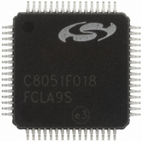
C8051F018-GQ Silicon Laboratories Inc, C8051F018-GQ Datasheet - Page 109

C8051F018-GQ
Manufacturer Part Number
C8051F018-GQ
Description
IC 8051 MCU 16K FLASH 64TQFP
Manufacturer
Silicon Laboratories Inc
Series
C8051F018r
Specifications of C8051F018-GQ
Program Memory Type
FLASH
Program Memory Size
16KB (16K x 8)
Package / Case
64-TQFP, 64-VQFP
Core Processor
8051
Core Size
8-Bit
Speed
25MHz
Connectivity
SMBus (2-Wire/I²C), SPI, UART/USART
Peripherals
Brown-out Detect/Reset, POR, PWM, Temp Sensor, WDT
Number Of I /o
32
Ram Size
1.25K x 8
Voltage - Supply (vcc/vdd)
2.8 V ~ 3.6 V
Data Converters
A/D 8x10b
Oscillator Type
Internal
Operating Temperature
-40°C ~ 85°C
Processor Series
C8051F0x
Core
8051
Data Bus Width
8 bit
Data Ram Size
1.25 KB
Interface Type
I2C/SMBus/SPI/UART
Maximum Clock Frequency
25 MHz
Number Of Programmable I/os
32
Number Of Timers
4
Operating Supply Voltage
2.8 V to 3.6 V
Maximum Operating Temperature
+ 85 C
Mounting Style
SMD/SMT
3rd Party Development Tools
PK51, CA51, A51, ULINK2
Development Tools By Supplier
C8051F005DK
Minimum Operating Temperature
- 40 C
On-chip Adc
8-ch x 10-bit
Lead Free Status / RoHS Status
Lead free / RoHS Compliant
Eeprom Size
-
Lead Free Status / Rohs Status
Lead free / RoHS Compliant
Other names
336-1197
Available stocks
Company
Part Number
Manufacturer
Quantity
Price
Company:
Part Number:
C8051F018-GQ
Manufacturer:
SiliconL
Quantity:
39
Company:
Part Number:
C8051F018-GQ
Manufacturer:
Silicon Laboratories Inc
Quantity:
10 000
Company:
Part Number:
C8051F018-GQR
Manufacturer:
Silicon Laboratories Inc
Quantity:
10 000
in an “off-line” state. In a multiple-master environment, the system controller should check the state of the
SLVSEL flag (SPI0CN.2) to ensure the bus is free before setting the MSTEN bit and initiating a data transfer.
15.3.
As shown in Figure 15.4, four combinations of serial clock phase and polarity can be selected using the clock
control bits in the SPI Configuration Register (SPI0CFG). The CKPHA bit (SPI0CFG.7) selects one of two clock
phases (edge used to latch the data). The CKPOL bit (SPI0CFG.6) selects between an active-high or active-low
clock. Both master and slave devices must be configured to use the same clock phase and polarity. Note: the SPI
should be disabled (by clearing the SPIEN bit, SPI0CN.0) while changing the clock phase and polarity.
The SPI Clock Rate Register (SPI0CKR) as shown in Figure 15.7 controls the master mode serial clock frequency.
This register is ignored when operating in slave mode.
109
C8051F018
C8051F019
Serial Clock Timing
MISO/MOSI
SCK
(CKPOL = 0, CKPHA = 0)
SCK
(CKPOL = 0, CKPHA = 1)
SCK
(CKPOL = 1, CKPHA = 0)
SCK
(CKPOL = 1, CKPHA = 1)
NSS
Figure 15.4. Data/Clock Timing Diagram
MSB
Bit 6
Rev. 1.2
Bit 5
Bit 4
Bit 3
Bit 2
Bit 1
LSB


