HW-SPAR3-SK-UNI-G Xilinx Inc, HW-SPAR3-SK-UNI-G Datasheet - Page 19
HW-SPAR3-SK-UNI-G
Manufacturer Part Number
HW-SPAR3-SK-UNI-G
Description
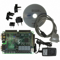
KIT STARTER SPARTAN-3
Manufacturer
Xilinx Inc
Series
Spartan-3r
Type
FPGA Configurationr
Datasheet
1.HW-SPAR3-SK-UNI-G.pdf
(64 pages)
Specifications of HW-SPAR3-SK-UNI-G
Contents
Board, Cable, Software, Datasheets and User Manual
For Use With/related Products
Spartan-3
Lead Free Status / RoHS Status
Lead free / RoHS Compliant
Other names
122-1521
Available stocks
Company
Part Number
Manufacturer
Quantity
Price


Switches and LEDs
Slide Switches
Push Button Switches
Spartan-3 FPGA Starter Kit Board User Guide
UG130 (v1.2) June 20, 2008
R
The Spartan
Figure
edge. The switches are labeled SW7 through SW0. Switch SW7 is the left-most switch, and
SW0 is the right-most switch. The switches connect to an associated FPGA pin, as shown in
Table
Table 4-1: Slider Switch Connections
When in the UP or ON position, a switch connects the FPGA pin to V
When DOWN or in the OFF position, the switch connects the FPGA pin to ground, a logic
Low. The switches typically exhibit about 2 ms of mechanical bounce and there is no active
debouncing circuitry, although such circuitry could easily be added to the FPGA design
programmed on the board. A 4.7KΩ series resistor provides nominal input protection.
The Spartan-3 Starter Kit board has four momentary-contact push button switches,
indicated as
board, toward the right edge. The switches are labeled BTN3 through BTN0. Push button
switch BTN3 is the left-most switch, BTN0 the right-most switch. The push button
switches connect to an associated FPGA pin, as shown in
appears in
Table 4-2: Push Button Switch Connections
Pressing a push button generates a logic High on the associated FPGA pin. Again, there is
no active debouncing circuitry on the push button.
The left-most button, BTN3, is also the default User Reset pin. BTN3 electrically behaves
identically to the other push buttons. However, when applicable, BTN3 resets the
provided reference designs.
Switch
FPGA Pin
Push Button
FPGA Pin
4-1. A detailed schematic appears in
1-2. The switches are located along the lower edge of the board, toward the right
Figure
®
-3 FPGA Starter Kit board has eight slide switches, indicated as
13
SW7
K13
in
BTN3 (User Reset)
A-2.
Figure
SW6
K14
L14
www.xilinx.com
1-2. These push buttons are located along the lower edge of the
SW5
J13
SW4
J14
Figure
BTN2
L13
A-2.
SW3
H13
Table
SW2
H14
BTN1
M14
4-2. A detailed schematic
SW1
G12
Chapter 4
CCO
, a logic High.
SW0
F12
BTN0
M13
11
in
19
Related parts for HW-SPAR3-SK-UNI-G
Image
Part Number
Description
Manufacturer
Datasheet
Request
R

Part Number:
Description:
STARTER KIT BUNDLE SPARTAN3/CPLD
Manufacturer:
Xilinx Inc
Part Number:
Description:
KIT HDWR FOR SPARTAN3/CPLD-JAPAN
Manufacturer:
Xilinx Inc

Part Number:
Description:
IC CPLD .8K 36MCELL 44-VQFP
Manufacturer:
Xilinx Inc
Datasheet:

Part Number:
Description:
IC CPLD 72MCRCELL 10NS 44VQFP
Manufacturer:
Xilinx Inc
Datasheet:

Part Number:
Description:
IC CPLD 1.6K 72MCELL 64-VQFP
Manufacturer:
Xilinx Inc
Datasheet:

Part Number:
Description:
IC CR-II CPLD 64MCELL 44-VQFP
Manufacturer:
Xilinx Inc
Datasheet:

Part Number:
Description:
IC CPLD 1.6K 72MCELL 100-TQFP
Manufacturer:
Xilinx Inc
Datasheet:

Part Number:
Description:
IC CR-II CPLD 64MCELL 56-BGA
Manufacturer:
Xilinx Inc
Datasheet:

Part Number:
Description:
IC CPLD 72MCRCELL 7.5NS 44VQFP
Manufacturer:
Xilinx Inc
Datasheet:
Part Number:
Description:
IC CR-II CPLD 64MCELL 100-VQFP
Manufacturer:
Xilinx Inc
Datasheet:
Part Number:
Description:
IC CPLD 1.6K 72MCELL 100-TQFP
Manufacturer:
Xilinx Inc
Datasheet:

Part Number:
Description:
IC CPLD 72MCRCELL 7.5NS 64VQFP
Manufacturer:
Xilinx Inc
Datasheet:
Part Number:
Description:
IC CPLD 1.6K 72MCELL 100-TQFP
Manufacturer:
Xilinx Inc
Datasheet:

Part Number:
Description:
IC CPLD 1.5K 64MCELL HP 44-VQFP
Manufacturer:
Xilinx Inc

Part Number:
Description:
IC CPLD 36MCRCELL 15NS 44PLCC
Manufacturer:
Xilinx Inc
Datasheet: