HW-SPAR3-SK-UNI-G Xilinx Inc, HW-SPAR3-SK-UNI-G Datasheet - Page 13
HW-SPAR3-SK-UNI-G
Manufacturer Part Number
HW-SPAR3-SK-UNI-G
Description
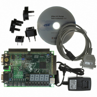
KIT STARTER SPARTAN-3
Manufacturer
Xilinx Inc
Series
Spartan-3r
Type
FPGA Configurationr
Datasheet
1.HW-SPAR3-SK-UNI-G.pdf
(64 pages)
Specifications of HW-SPAR3-SK-UNI-G
Contents
Board, Cable, Software, Datasheets and User Manual
For Use With/related Products
Spartan-3
Lead Free Status / RoHS Status
Lead free / RoHS Compliant
Other names
122-1521
Available stocks
Company
Part Number
Manufacturer
Quantity
Price


Write Enable and Output Enable Control Signals
Write Enable and Output Enable Control Signals
SRAM Data Signals, Chip Enables, and Byte Enables
Spartan-3 FPGA Starter Kit Board User Guide
UG130 (v1.2) June 20, 2008
Both 256Kx16 SRAMs share common output enable (OE#) and write enable (WE#) control
lines, as shown in
Connector (refer to
Table 2-2: External SRAM Control Signal Connections to Spartan-3 FPGA
The data signals, chip enables, and byte enables are dedicated connections between the
FPGA and SRAM.
IC10 in
SRAM, drive the associated chip enable pin High.
Table 2-3: SRAM IC10 Connections
UB1 (upper byte enable IC10)
LB1 (lower byte enable IC10)
CE1 (chip enable IC10)
Figure
Signal
WE#
OE#
Signal
A-8.
IO15
IO14
IO13
IO12
IO10
IO11
IO9
IO8
IO7
IO6
IO5
IO4
IO3
IO2
IO1
IO0
Table
Table 2-3
Table 2-4
“Expansion Connectors,” page
2-2. These control signals also connect to the A1 Expansion
www.xilinx.com
shows the FPGA pin connections to the SRAM designated
shows the FPGA pin connections to SRAM IC11. To disable an
FPGA Pin
K4
G3
FPGA Pin
H1
D3
N7
R1
P1
L2
P8
B1
C1
C2
R5
T5
R6
T8
P7
T4
F2
P6
J2
A1 Expansion Connector Pin
A1 Expansion Connector Pin
47).
18
16
19
17
15
13
11
9
7
5
13
R
Related parts for HW-SPAR3-SK-UNI-G
Image
Part Number
Description
Manufacturer
Datasheet
Request
R

Part Number:
Description:
STARTER KIT BUNDLE SPARTAN3/CPLD
Manufacturer:
Xilinx Inc
Part Number:
Description:
KIT HDWR FOR SPARTAN3/CPLD-JAPAN
Manufacturer:
Xilinx Inc

Part Number:
Description:
IC CPLD .8K 36MCELL 44-VQFP
Manufacturer:
Xilinx Inc
Datasheet:

Part Number:
Description:
IC CPLD 72MCRCELL 10NS 44VQFP
Manufacturer:
Xilinx Inc
Datasheet:

Part Number:
Description:
IC CPLD 1.6K 72MCELL 64-VQFP
Manufacturer:
Xilinx Inc
Datasheet:

Part Number:
Description:
IC CR-II CPLD 64MCELL 44-VQFP
Manufacturer:
Xilinx Inc
Datasheet:

Part Number:
Description:
IC CPLD 1.6K 72MCELL 100-TQFP
Manufacturer:
Xilinx Inc
Datasheet:

Part Number:
Description:
IC CR-II CPLD 64MCELL 56-BGA
Manufacturer:
Xilinx Inc
Datasheet:

Part Number:
Description:
IC CPLD 72MCRCELL 7.5NS 44VQFP
Manufacturer:
Xilinx Inc
Datasheet:
Part Number:
Description:
IC CR-II CPLD 64MCELL 100-VQFP
Manufacturer:
Xilinx Inc
Datasheet:
Part Number:
Description:
IC CPLD 1.6K 72MCELL 100-TQFP
Manufacturer:
Xilinx Inc
Datasheet:

Part Number:
Description:
IC CPLD 72MCRCELL 7.5NS 64VQFP
Manufacturer:
Xilinx Inc
Datasheet:
Part Number:
Description:
IC CPLD 1.6K 72MCELL 100-TQFP
Manufacturer:
Xilinx Inc
Datasheet:

Part Number:
Description:
IC CPLD 1.5K 64MCELL HP 44-VQFP
Manufacturer:
Xilinx Inc

Part Number:
Description:
IC CPLD 36MCRCELL 15NS 44PLCC
Manufacturer:
Xilinx Inc
Datasheet: