DK-NIOS-2C35N Altera, DK-NIOS-2C35N Datasheet - Page 14
DK-NIOS-2C35N
Manufacturer Part Number
DK-NIOS-2C35N
Description
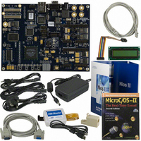
NIOS II KIT W/CYCLONE II EP2C35N
Manufacturer
Altera
Series
Cyclone® IIr
Type
Nios®IIr
Specifications of DK-NIOS-2C35N
Contents
Eval Board, Design Apps, Software, Cables and Accessories
For Use With/related Products
Cyclone ll 2C35N
Lead Free Status / RoHS Status
Lead free / RoHS Compliant
Other names
544-1698
DK-NIOS-2C35N
DK-NIOS-2C35N
Available stocks
Company
Part Number
Manufacturer
Quantity
Price


Board Components
2–2
Nios Development Board Cyclone II Edition
Memory
U74
U5, LED7
U63
Connections & Interfaces
U4, RJ1
J19
PROTO1 (J11, J12, J13) Expansion prototype
PROTO2 (J15, J16, J17) Expansion prototype
CON3
JH1, JH2
J25
TP1 – TP8
J24
J5
J27
Configuration & Reset
U3
U69
SW8
Table 2–1. Nios Development Board, Cyclone II Edition Components & Interfaces (Continued)
Board Designation
SSRAM memory
Flash memory
DDR SDRAM memory
Ethernet MAC/PHY
Serial connector
connector
connector
CompactFlash connector
PMC connector
Mictor connector
Test Points
JTAG connector
JTAG connector
EPCS configuration header
MAX Configuration controller Altera MAX EPM7256AE device used to configure
Serial configuration device
CPU Reset button
Name
Reference Manual
2 Mbytes of synchronous SRAM.
16 Mbytes of nonvolatile memory for use by both the
FPGA and the configuration controller. LED7 lights
whenever the flash chip-enable is asserted.
32 Mbytes of DDR SDRAM.
10/100 Ethernet MAC/PHY chip connected to an RJ-
45 Ethernet connector.
RS-232 serial connector with 5 V-tolerant buffers.
Supports all RS-232 signals.
Expansion headers connecting to 41 I/O pins on the
FPGA. Supplies 3.3V and 5.0V for use by a daughter
card.
Expansion headers connecting to 41 I/O pins on the
FPGA. Supplies 3.3V and 5.0V for use by a daughter
card.
CompactFlash connector for memory expansion.
Expansion connector for a PCI mezzanine card.
Mictor connector providing access to 27 I/O pins on
the FPGA. Allows debugging Nios II systems using a
First Silicon Solutions (FS2) debug probe.
Test points providing access to eight FPGA I/O pins.
JTAG connection to the FPGA allowing hardware
configuration using the
Quartus
Nios II IDE.
JTAG connection to the MAX
controller.
Connects to the EPCS serial configuration device for
in-system programming.
the FPGA from flash memory.
Altera EPCS64 low-cost serial configuration device to
configure the FPGA.
Push-button switch to reboot the Nios II processor
configured in the FPGA.
®
II software and software debug using the
Description
®
configuration
Altera Corporation
May 2007
Related parts for DK-NIOS-2C35N
Image
Part Number
Description
Manufacturer
Datasheet
Request
R

Part Number:
Description:
NIOS II KIT W/STRATIX II EP2S60N
Manufacturer:
Altera
Datasheet:

Part Number:
Description:
CYCLONE II STARTER KIT EP2C20N
Manufacturer:
Altera
Datasheet:

Part Number:
Description:
KIT DEV NIOS II CYCLONE III ED.
Manufacturer:
Altera
Datasheet:

Part Number:
Description:
KIT DEV MAXII W/EPM 1270N
Manufacturer:
Altera
Datasheet:

Part Number:
Description:
DK-SLSR30-300N EZS RCVR NI HSG 30mm X 300mm NO PKG
Manufacturer:
BANNER ENGINEERING


Part Number:
Description:
CPLD, EP610 Family, ECMOS Process, 300 Gates, 16 Macro Cells, 16 Reg., 16 User I/Os, 5V Supply, 35 Speed Grade, 24DIP
Manufacturer:
Altera Corporation
Datasheet:
Part Number:
Description:
CPLD, EP610 Family, ECMOS Process, 300 Gates, 16 Macro Cells, 16 Reg., 16 User I/Os, 5V Supply, 15 Speed Grade, 24DIP
Manufacturer:
Altera Corporation
Datasheet:
Part Number:
Description:
Manufacturer:
Altera Corporation
Datasheet:
Part Number:
Description:
CPLD, EP610 Family, ECMOS Process, 300 Gates, 16 Macro Cells, 16 Reg., 16 User I/Os, 5V Supply, 30 Speed Grade, 24DIP
Manufacturer:
Altera Corporation
Datasheet:
Part Number:
Description:
High-performance, low-power erasable programmable logic devices with 8 macrocells, 10ns
Manufacturer:
Altera Corporation
Datasheet:
Part Number:
Description:
High-performance, low-power erasable programmable logic devices with 8 macrocells, 7ns
Manufacturer:
Altera Corporation
Datasheet:
Part Number:
Description:
Classic EPLD
Manufacturer:
Altera Corporation
Datasheet:
Part Number:
Description:
High-performance, low-power erasable programmable logic devices with 8 macrocells, 10ns
Manufacturer:
Altera Corporation
Datasheet: